Semiconductor structure and forming method thereof

A semiconductor and entity technology, applied in semiconductor devices, semiconductor/solid-state device manufacturing, semiconductor/solid-state device components, etc., can solve problems such as coarse side effects of the upper cover layer, and achieve the effect of improving mechanical strength and increasing impedance

Inactive Publication Date: 2007-09-05
TAIWAN SEMICON MFG CO LTD
View PDF0 Cites 13 Cited by
  • Summary
  • Abstract
  • Description
  • Claims
  • Application Information

AI Technical Summary

Problems solved by technology

This would result in thicker edges on the cap layer and undesired side effects

Method used


Image

  • Semiconductor structure and forming method thereof
  • Semiconductor structure and forming method thereof
  • Semiconductor structure and forming method thereof

Examples


Embodiment Construction

[0045] A preferred embodiment of the present invention is illustrated by FIGS. 1 to 9, wherein like reference numerals indicate similar elements.

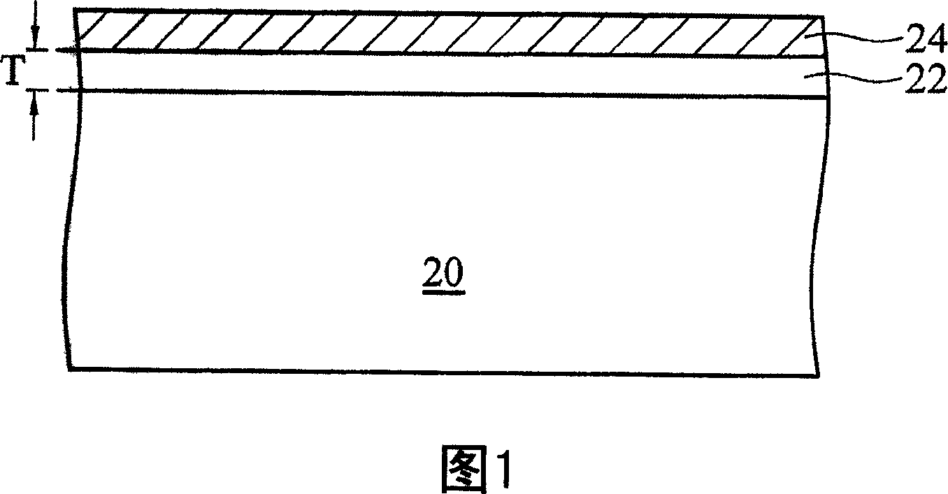
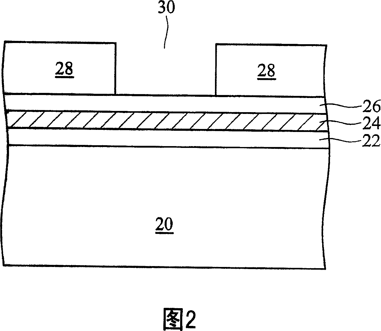
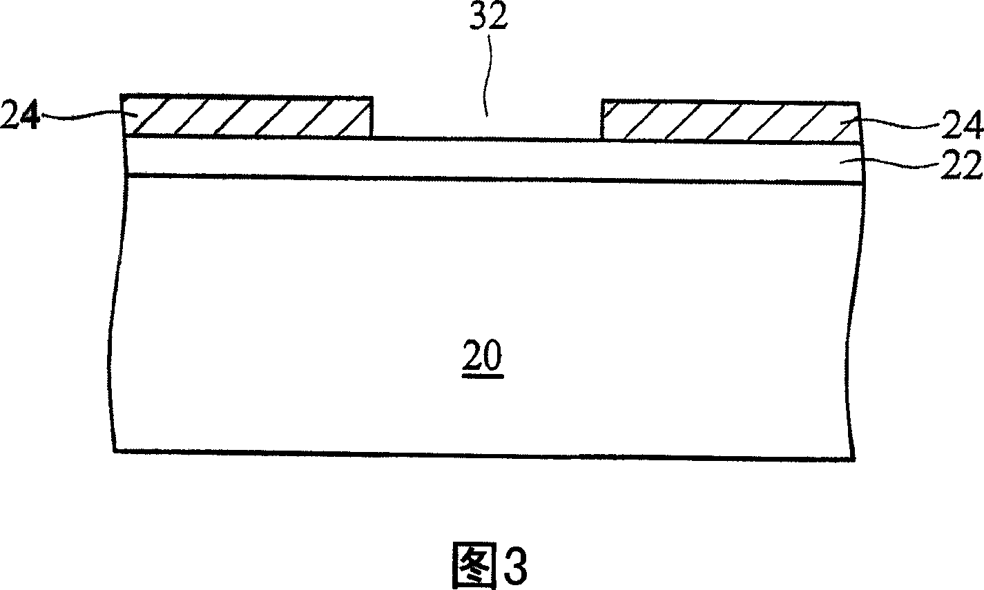
[0046] Please refer to FIG. 1 , which shows an upper cap layer 22 and a metal hard mask 24 formed on a low-k dielectric layer 20, which are used to insulate underlying components (not shown) and to be formed later. metal wires. The low-k dielectric layer 20 has a low k, preferably less than 3.5 and more preferably less than 2.5, and is therefore sometimes referred to as an extremely low-k dielectric material. The low-k dielectric layer 20 may include carbon-doped silicon oxide, fluorine-doped silicon oxide, organic low-k material, porous low-k material, and the like. The low-k dielectric layer 20 can be formed by, for example, spin coating, chemical vapor deposition, plasma enhanced chemical vapor deposition, low pressure chemical vapor deposition, and other known deposition techniques.

[0047] A capping layer 22 is then formed ...


PUM

PropertyMeasurementUnit
thicknessaaaaaaaaaa
thicknessaaaaaaaaaa

Abstract

The present invention discloses a semiconductor structure and a method for forming the semiconductor structure; the semiconductor structure comprises: a dielectric layer with a low dielectric constant; an top cover layer on the dielectric layer, wherein, the top cover layer is made of a material formed by a compound group selected from CNx, SiCN, SiCO, SiC, and their mixtures; a dielectric substance in the dielectric layer; and, a metal conductor, which is in the dielectric layer and covers the dielectric substance; in addition, the body of the metal conductor contacts the dielectric substance. The semiconductor structure and the method provided in the present invention are characterized in stability under high-temperature and high electron breakdown field, can improve impedance to thermal circulation and electric power applied, and improve mechanical strength of the semiconductor structure, without any additional manufacturing cost.

Description

technical field [0001] The present invention relates to semiconductor device interconnections, and more particularly to materials used in interconnects overlying low-k dielectric materials. Background technique [0002] High density integrated circuits such as very large scale integrated circuits (VLSI) typically have multiple metal interconnections to form three-dimensional (3D) routing structures. The purpose of using multiple metal interconnects is to properly connect closely stacked components. As the integration level of components increases, a parasitic capacitance effect (parasitic capacitance) occurs between metal interconnections. In order to reduce the parasitic capacitance and increase the transmission speed between metal interconnections, low-k dielectric materials (low-k dielectric) are usually used as the inter-layer dielectric layer (inter-layer dielectric, ILD) and metal interlayer dielectric. layer (inter-metal dielectric, IMD). [0003] One of the most c...

Claims


Application Information

Patent Timeline
Patent Type & Authority Applications(China)
IPC IPC(8): H01L23/522H01L23/532H01L21/768
CPCH01L21/76811H01L23/53295H01L21/76829H01L21/76832H01L21/76813H01L2924/3011H01L23/5329H01L2924/0002H01L2924/00
Inventor 张惠林卢永诚包天一
Owner TAIWAN SEMICON MFG CO LTD
Why Eureka
Try Eureka