Manufacturing method of light guiding board/ light guiding film mould core

A manufacturing method and technology for light guide plates, which are applied in manufacturing tools, optics, light guides, etc., can solve the problems of slow market adaptability, increased difficulty in implementation, and complicated manufacturing processes, and can shorten the production cycle, sample time, and process. simple effect

Inactive Publication Date: 2007-09-12
SVG TECH GRP CO LTD +1
View PDF1 Cites 33 Cited by
  • Summary
  • Abstract
  • Description
  • Claims
  • Application Information

AI Technical Summary

Problems solved by technology

The similarities of the above methods are that the manufacturing process is complicated and the cost is high. At the same time, the performance of the light guide plate can only be tested after the subsequent injection molding process is completed. Therefore, its market adaptability is relatively slow.
[0004] In addition, with the development of backlight modules in the direction of thinning, the requi

Method used


Image

  • Manufacturing method of light guiding board/ light guiding film mould core
  • Manufacturing method of light guiding board/ light guiding film mould core
  • Manufacturing method of light guiding board/ light guiding film mould core

Examples


Embodiment 1

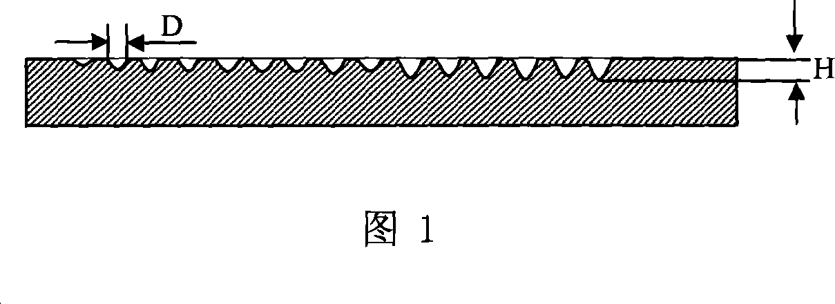
[0020] Embodiment 1: High-power diode-pumped solid-state laser: tripled frequency 351nm / 355nm or quadrupled frequency 263nm / 266nm, single pulse energy > 3mJ. The laser beam emitted by the laser passes through the beam shaping system, then collimates and focuses the optical path, and converges on the surface of the light guide plate substrate placed on the platform, such as PMMA and PC. Microstructure dots with different depths can be obtained by changing the laser energy or changing the etching time on the surface of the light guide plate substrate. Accompanying drawing 1 is the sectional view of the light guide plate of the PC substrate with the same diameter and different etching depths. In this embodiment, the dot diameter D=50um, and the dot depth H=5um-15um.

Embodiment 2

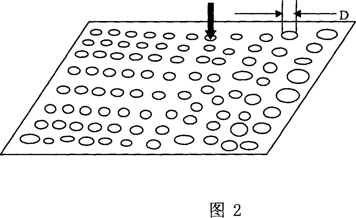
[0021] Embodiment 2: High-power diode-pumped solid-state laser: tripled frequency 351nm / 355nm or quadrupled frequency 263nm / 266nm, single pulse energy > 3mJ. The laser beam emitted by the laser passes through the beam shaping system, then collimates and focuses the optical path, and converges on the surface of the light guide plate substrate placed on the platform, such as PMMA and PC. The spot shape or light intensity distribution can be changed through the beam shaping system, so that dots with different surface shapes and groove shapes can be obtained. Accompanying drawing 2 is the top view of the light guide plate with circular microlens groove-shaped light guide dots after etching, and the dot diameter D=10-100um. While changing the dot diameter, the shape of the light spot and the energy of the laser beam can also be changed in real time to make light guide dots of different shapes and depths, which will not be described in detail.

Embodiment 3

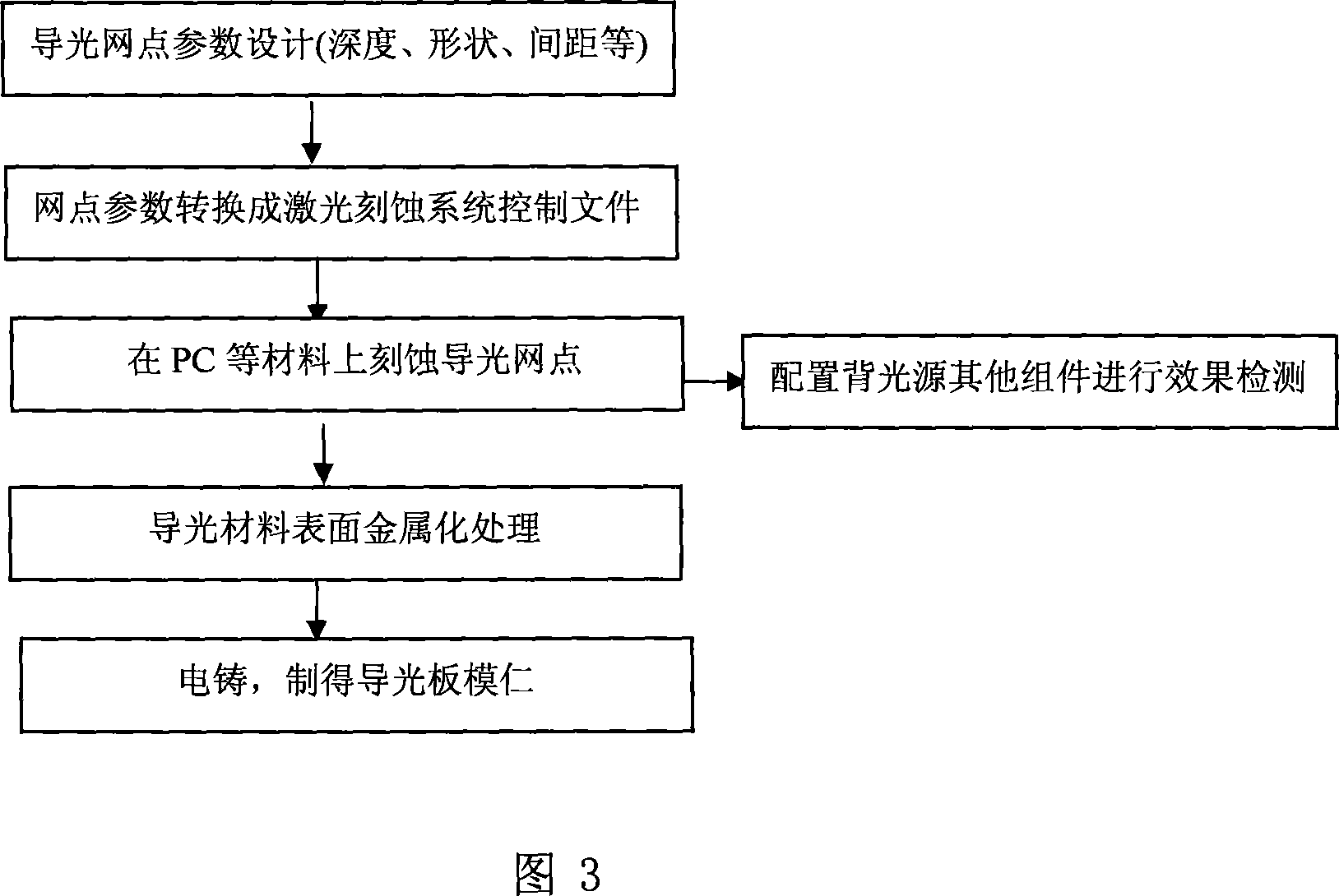
[0022] Embodiment 3: Taking the production of a side-emitting light guide plate (film) used in a mobile phone keyboard backlight module as an example, refer to the accompanying drawing 3, and introduce the process steps of making the mold core of the light guide plate (film) according to the present invention in detail. (1) Design and determine the light guide area according to the application requirements, draw the pattern, use the dot design software to design the dot distribution of the light guide area according to the characteristics of the light source, use the optical simulation software to evaluate the luminance and uniformity of the designed dots, and make dots for the dots further optimization. Determine the dot size, depth and other parameters. (2) Convert the designed dot distribution and dot parameters into controllable files of laser etching equipment. (3) Adjust the optical path of the laser etching equipment, set the corresponding parameters, and perform etchi...


PUM

PropertyMeasurementUnit
Diameteraaaaaaaaaa
Depthaaaaaaaaaa
Diameteraaaaaaaaaa

Abstract

This invention discloses a method of producing lightguide plate/ lightguide membrane mode kernel, according to the lightguide-demand, form lightguide network structure on the surface of the lightguide substrate, the features are: use of high-power pulsed lasers, through beam shaping, collimate light focused directly on the substrate surface etching lightguide networks, obtain lightguide plate monomeric unit, metallizing the surface of the lightguide plate monomeric unit etched, Further electroforming, meanwhile, In nickel metal deposited on the surface, make nickel metal deposited and lightguide substrate separated, then get the lightguide plate/ lightguide membrane mode kernel needed. At the same time, the lightguide plate monomeric unit etched can be used as backlight module, dispose other backlight module; the invention can detect the lightguide performance. This invention can be carried out rapid for evaluating the design of networks and providing samples, after metal processing and electroforming process, the lightguide plate/ lightguide membrane mode kernel can be made, greatly reducing the production cycle, simplify the process and reduce the cost ,have a faster market response capability.

Description

technical field [0001] The invention relates to a method for manufacturing a mold core for making a light guide plate / light guide film, in particular to a non-printing method for manufacturing an ultra-thin light guide film mold core with an ultrafine light guide structure. Background technique [0002] In the backlight modules of LCD displays, mobile phones, digital cameras, lighting, etc., the light guide plate is one of the key components. At present, the manufacturing methods of light guide plates can be divided into printing methods and non-printing methods. The printing method is to use high-scattering light source materials (such as SiO 2 &TiO 2 ) of the printing material, properly distributed on the bottom surface of the light guide plate, through the nature of the printing material to absorb and re-diffuse the light source, destroy the internal propagation caused by the total reflection effect, so that the light is emitted from the front a...

Claims


Application Information

Patent Timeline
IPC IPC(8): G02B6/00B23K26/00H01S3/00G02F1/1335B23K26/362
Inventor 周小红陈林森魏国军解正东吴智华
Owner SVG TECH GRP CO LTD
Why Eureka
Try Eureka