Method for manufacturing substrate of embedded element

A technology of embedded components and manufacturing methods, which is applied in the direction of semiconductor/solid-state device manufacturing, electrical components, and printed circuits connected with non-printed electrical components. Components are embedded in the substrate, affecting the alignment of embedded components and contacts, etc.

Inactive Publication Date: 2007-09-19
ADVANCED SEMICON ENG INC
View PDF0 Cites 14 Cited by
  • Summary
  • Abstract
  • Description
  • Claims
  • Application Information

AI Technical Summary

Problems solved by technology

However, in the current technology using embedded electronic components, when the circuit layer and the insulating layer are pressed together to form the substrate, since the insulating layer is cured at a high temperature, most of them are in a cured state that is not easily deformed, so it is easy to cause internal There are still many unfilled gaps between the buried components and the insulating layer. These gaps not only easily affect the bonding between the substrate and the embedded components during pressing, but also affect the alignment of the embedded components and contacts during pressing.
In addition, in a circuit substrate with a single insulating layer, the thickness of the insulating layer is usually smaller than that of the embedded components, which easily causes problems such as the inability to embed the components in the substrate.

Method used


Image

  • Method for manufacturing substrate of embedded element
  • Method for manufacturing substrate of embedded element
  • Method for manufacturing substrate of embedded element

Examples


no. 1 example

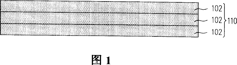
[0031] FIG. 1 to FIG. 10 are schematic diagrams sequentially illustrating a method for manufacturing a substrate with embedded components according to a first embodiment of the present invention. First, as shown in FIG. 1 , a core layer 110 is provided, and the core layer 110 is composed of a multi-layer first insulating layer 102 . Wherein, the form of the first insulating layer 102 can be a semi-cured state between liquid and solid, and its material is, for example, glass-oxygen resin (FR-4, FR-5), bismaleic acid imide Impregnation (preprag) insulating materials such as amine (Bismaleimide-Triazine, BT) or epoxy resin (epoxy resin). Since the first insulating layer 102 is in a semi-cured state, the first insulating layer 102 has both a fluid deformation property and a solid particle aggregation property, and the first insulating layer 102 is easily thermoset by being heated.

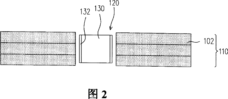
[0032] Next, as shown in FIG. 2, a buried hole is formed in the core layer 110, such as a through ...

no. 2 example

[0043] FIG. 11 to FIG. 20 are schematic diagrams sequentially illustrating a method for manufacturing a substrate with embedded components according to the second embodiment of the present invention. Wherein, the substrate manufacturing process of the embedded components in FIGS. 11 to 14 is the same as the substrate manufacturing process of the embedded components in FIGS. 1 to 4 in the first embodiment, and will not be repeated here.

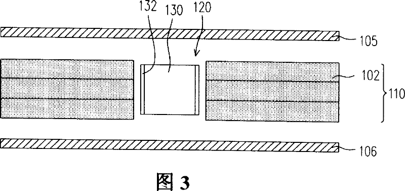
[0044] Please refer to FIG. 15 and FIG. 16 at the same time, so that the embedded element 130 is electrically connected to the metal layer 105 . Wherein, the step of electrically conducting the embedded element 130 and the metal layer 105 may be to use laser drilling first, and then form a drill hole 140 in the core layer 110, and expose the electrode 132 of the embedded element 130, as shown in FIG. 15 shown. Then, electroplating is used to fill the drilled hole 140 with a conductive material, so that the conductive column 142 is formed in t...


PUM


Abstract

The invention discloses a method for making substrate embedded with element. The method includes: firstly, providing a core layer comprised by stacking plural insulation layers in partially curing state; and then, forming embedding hole on the core layer and disposing an inner embedded element with at least one electrodes in the embedding hole; respectively forming metallic layers on upper and lower surfaces, and pressing the core layer and the two metallic layer together to fill the insulation layer into the embedding hole and coat the periphery surface of the embedded element; at last, respectively patterning the metallic layers of the upper and lower surface of the core layer to from a first signal layer and a second signal layer on both upper and lower surfaces of the core layer thereby electrically connecting the embedded element to realize electrical connection of the electrode of the embedded element and the first signal layer.

Description

technical field [0001] The invention relates to a manufacturing method of a substrate, in particular to a manufacturing method of a substrate of an embedded component. Background technique [0002] Usually, a circuit substrate is mainly composed of multiple layers of patterned circuit layers and insulating layers (dielectric layers) stacked alternately. The patterned circuit layer is defined by a copper foil layer through lithography and etching manufacturing processes, and the insulating layer is arranged between the patterned circuit layers to isolate the patterned circuit layer. In addition, the overlapping patterned circuit layers are electrically connected to each other through Plating Through Holes (PTH) or conductive vias penetrating the insulating layer. Finally, arrange various electronic components (active components, passive components) on the surface of the circuit substrate, and achieve the purpose of electrical signal propagation through the circuit design of ...

Claims


Application Information

Patent Timeline
IPC IPC(8): H01L21/60H01L23/488H05K3/32H05K1/18
Inventor 洪清富林素玉薛彬佑
Owner ADVANCED SEMICON ENG INC
Why Eureka
Try Eureka