Method for producing semiconductor device

A manufacturing method and semiconductor technology, applied in the fields of semiconductor/solid-state device manufacturing, semiconductor devices, electrical components, etc., can solve the problems of device performance degradation and difficult control of LDD depth, and achieve the elimination of concave phenomenon, good etching selectivity, and simplification. The effect of the etching process

Inactive Publication Date: 2007-10-10
SEMICON MFG INT (SHANGHAI) CORP +1
View PDF1 Cites 22 Cited by
  • Summary
  • Abstract
  • Description
  • Claims
  • Application Information

AI Technical Summary

Problems solved by technology

However, for the process node of 65nm or even 45nm, the thickness of the gate oxide layer is only about 60 Ȧ, it will be etched away and the lateral

Method used


Image

  • Method for producing semiconductor device
  • Method for producing semiconductor device
  • Method for producing semiconductor device

Examples


Embodiment Construction

[0027] In order to make the above objects, features and advantages of the present invention more comprehensible, specific implementations of the present invention will be described in detail below in conjunction with the accompanying drawings.

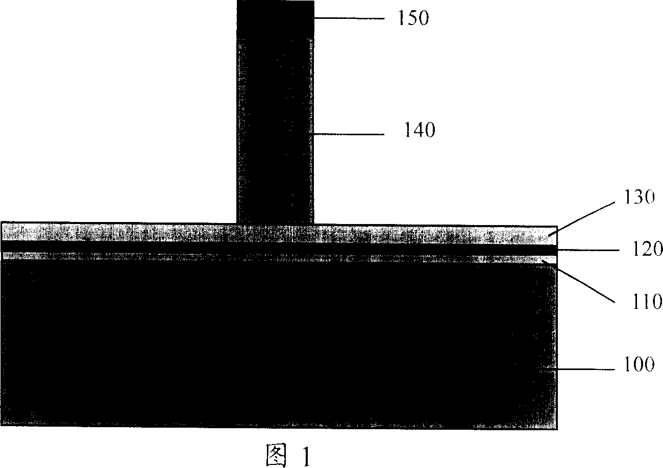
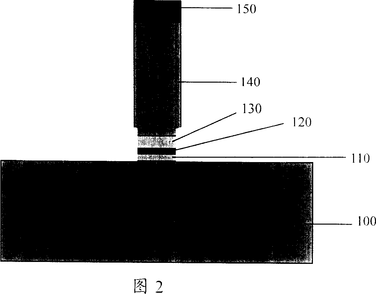
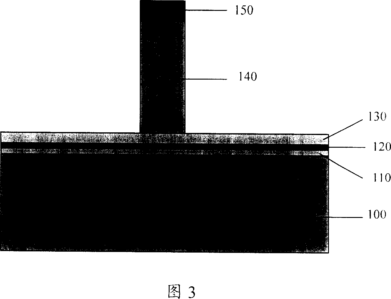
[0028] The invention discloses a method for manufacturing a semiconductor gate structure. The etching of the ONO stacked structure of SONOS devices with a thickness of 65nm and below has high precision. The method can be used to manufacture next-generation low-voltage high-density non-volatile semiconductor flash memory devices.

[0029] FIG. 3 and FIG. 4 are schematic diagrams of the ONO stack structure of the SONOS device illustrating the manufacturing method of the semiconductor gate structure of the present invention. SONOS (silicon-oxide-nitirde-oxide-silicon silicon-oxide-nitride-oxide-silicon) device is a new generation of non-volatile large-capacity semiconductor storage device, and its core structure is a polysilicon gate 140...


PUM


Abstract

When etching ONO laminated construction of SONOS parts, the method uses mixed gas of carbon tetrafluoride (CF4) and fluoroform (CHF3) as main etching gas instead of mixed gas of HBr and C2F6, and uses CHF3 as over etching gas instead of mixed gas of CH2F2/SF6. Using mixed gas of CF4 and CHF3 accomplishes main etching and over etching step for one time so as to simplify etching technique. Based on good etching selectivity and suitable etching speed, the method controls and buffers effect for etching ONO laminated construction by plasma of etching gas. In procedure for etching wafer thin oxidizing layer of grid electrode, the method is capable of controlling etching depth accurately, stopping etching at oxidation surface at low layer of ONO. Moreover, the method eliminates concave phenomena at sidewall and root part of polysilicon gate caused by transversal etching.

Description

technical field [0001] The invention relates to the technical field of semiconductor integrated circuit manufacturing, in particular to a method for manufacturing a semiconductor SONOS (silicon-oxide-nitirde-oxide-silicon silicon-oxide-nitride silicon-oxide-silicon) device gate structure. Background technique [0002] With the rapid development of semiconductor manufacturing technology, in order to achieve faster computing speed, larger data storage capacity and more functions of semiconductor devices, semiconductor wafers are developing towards higher component density and high integration. SONOS (silicon-oxide-nitirde-oxide-silicon) devices, as a new generation of low-voltage, high-density non-volatile semiconductor flash memory devices, have attracted increasing attention due to their excellent scaling characteristics . The core structure of the SONOS device is an oxide-nitirde-oxide ONO stack structure formed between the polysilicon gate and the surface of the silicon s...

Claims


Application Information

Patent Timeline
IPC IPC(8): H01L21/28H01L21/336H01L21/3065H01L21/311
Inventor 张海洋刘燕丽
Owner SEMICON MFG INT (SHANGHAI) CORP
Why Eureka
Try Eureka