Silicon lining bottom plane LED integrated chip and producing method

A technology of integrated chip and silicon substrate, which is applied in the field of silicon substrate planar LED integrated chip and its manufacturing, can solve the problems of easy short circuit of integrated chip and inability to realize series connection, etc., and achieve reduction of operation time of bonding process, low cost, The effect of occupying a small area

Inactive Publication Date: 2007-10-10
NANKER GUANGZHOU SEMICON MFG
View PDF0 Cites 14 Cited by
  • Summary
  • Abstract
  • Description
  • Claims
  • Application Information

AI Technical Summary

Problems solved by technology

Since the commonly used LED circuit boards are all aluminum substrates, and the aluminum substrate itself is a conductor, it is very easy to short circuit during the processing of integrated chips and cannot be connected in series.

Method used


Image

  • Silicon lining bottom plane LED integrated chip and producing method
  • Silicon lining bottom plane LED integrated chip and producing method
  • Silicon lining bottom plane LED integrated chip and producing method

Examples


Embodiment 1

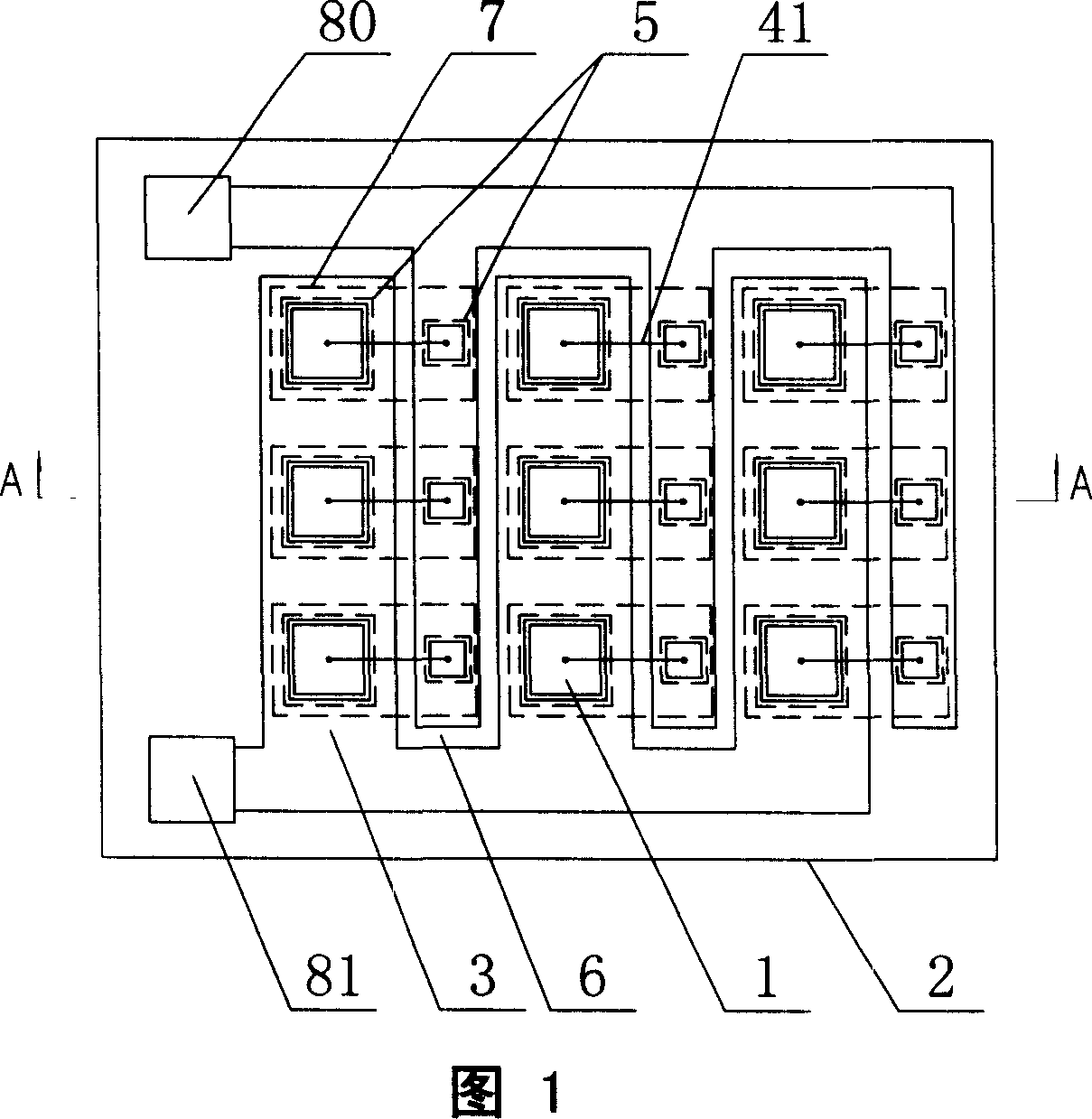
[0053] As shown in Fig. 1, Fig. 2, and Fig. 13, the silicon substrate planar LED integrated chip of this embodiment is a formally mounted LED integrated chip, which includes nine LED bare chips 1 and a silicon substrate 2, and the LED bare chip 1 includes Gallium arsenide (GaAs) substrate 10 and N-type epitaxial layer 11, P-type epitaxial layer 12, of course, the substrate 10 can also be a silicon carbide (SiC) substrate, that is, the LED bare chip 1 is a single electrode Chip, the silicon substrate 2 is an N-type silicon substrate, and the top surface of the silicon substrate 2 has two separate deposited metal layers 3 at each of the LED bare chips 1, and the LED bare chips 1 are mounted Welded on each of the metal layers 3, that is, the substrate 10 is directly welded on the metal layer 3, and the P-type epitaxial layer 12 is correspondingly welded on an adjacent metal layer 3 through a metal wire 41 , the silicon substrate 2 has a P-type well region 7 at each of the LED bar...

Embodiment 2

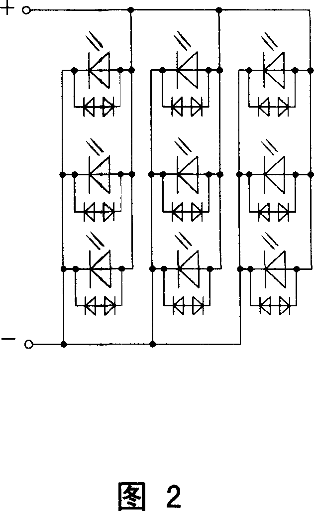
[0062] As shown in Figure 3, Figure 4, and Figure 14, the difference between this embodiment and Embodiment 1 lies in: the connection mode between the LED bare chips 1 through the metal layer 3 - each of the LED chips 1 in this embodiment The LED bare chips 1 are connected in series, that is, all the LED bare chips 1 between the anode contact 80 and the cathode contact 81 are connected in series.

[0063] The remaining features of this embodiment are the same as those of Embodiment 1.

Embodiment 3

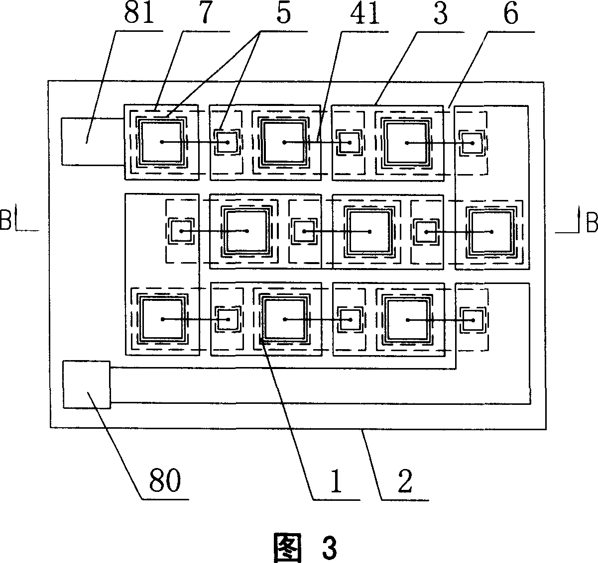
[0065] As shown in Fig. 5, Fig. 6, and Fig. 15, the difference between this embodiment and Embodiment 1 lies in: the connection method between each of the LED bare chips 1 through the metal layer 3—— The above-mentioned LED bare chips 1 are connected in series every three to form a group, and then the three groups are connected in parallel.

[0066] The remaining features of this embodiment are the same as those of Embodiment 1.


PUM


Abstract

The integrated chip includes LED bare chips, and silicon substrate. LED bare chip includes substrate, N type epitaxial layer, and P type epitaxial layer. There are two separated deposited metal layers at each LED bare chip on each top face of silicon substrate. Trap area is located at LED bare chip on silicon substrate. Adulterated isolation layer is located at bonding pad of each metal layer and silicon substrate. The isolation layer is within the trap area. Barrier layer is setup between metal layers corresponding to each LED bare chip. The method includes steps for forming barrier layer, trap area, isolation layer, metal layer, and packaging LED. The invention is applicable to area for integrating LEDs.

Description

technical field [0001] The invention relates to a silicon substrate planar LED integrated chip and a manufacturing method thereof. Background technique [0002] Front-mount chip technology is a traditional microelectronic packaging technology, which is mature and widely used. At present, the vast majority of LEDs are formal-mounted LEDs. Whether the substrate of the LED bare chip is gallium arsenide or silicon carbide, a layer of metal is plated on the outside of the substrate as an N-type electrode, and it is also used for heat dissipation. A bracket with a reflective cup is used as the cathode, and the P-type epitaxial layer on it is welded to the anode lead through a metal wire. Since the top of the bare chip and the substrate surface are used as one end of the electrode, it is commonly called "single electrode chip". In addition to the above-mentioned single-electrode bare LED chip (the front and back of the chip have an electrode), some LED ba...

Claims


Application Information

Patent Timeline
Patent Type & Authority Applications(China)
IPC IPC(8): H01L25/00H01L25/075H01L23/488H01L21/607
CPCH01L2224/49107H01L2224/45147H01L2224/48091H01L2224/45124H01L2224/45144H01L2924/01015H01L2924/00014H01L2924/00
Inventor 吴纬国
Owner NANKER GUANGZHOU SEMICON MFG
Why Eureka
Try Eureka