GaAs/AlGaAs/InGaAs dual color focal plane detector

A focal plane detector, device chip technology, applied in semiconductor devices, electrical components, circuits, etc., can solve problems such as increased process difficulty, and achieve the effect of simple material structure

Inactive Publication Date: 2007-10-17
SHANGHAI INST OF TECHNICAL PHYSICS - CHINESE ACAD OF SCI
View PDF0 Cites 18 Cited by
  • Summary
  • Abstract
  • Description
  • Claims
  • Application Information

AI Technical Summary

Problems solved by technology

If the diffraction grating is deeply etched at this time, the difficulty of the process will be greatly increased, and it is difficult to do it with the general conventional process. At present, there are only 2-3 laboratories in the world that can do such deep etching.

Method used


Image

  • GaAs/AlGaAs/InGaAs dual color focal plane detector
  • GaAs/AlGaAs/InGaAs dual color focal plane detector
  • GaAs/AlGaAs/InGaAs dual color focal plane detector

Examples


Embodiment Construction

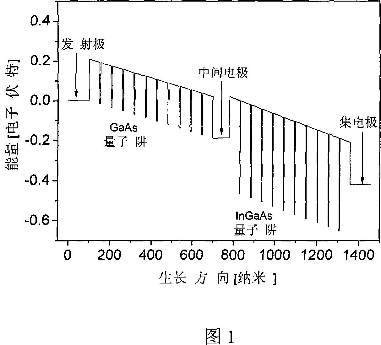
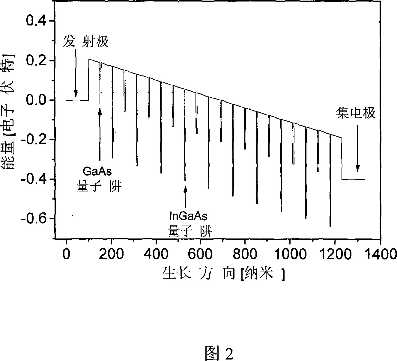
[0031] Taking the mid-wave infrared band with peak detection wavelength around 4.5 μm and the long-wave infrared band around 9.3 μm as examples, the specific implementation of the present invention will be further described in detail in conjunction with the accompanying drawings.

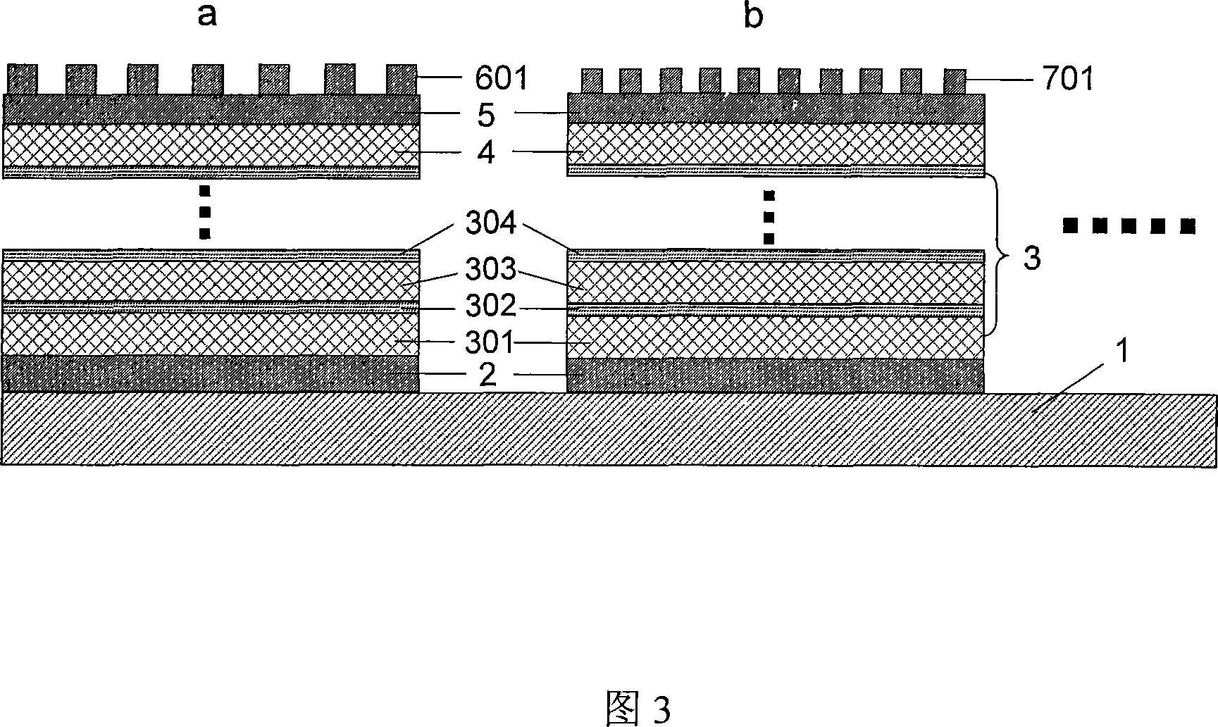
[0032] First, on the GaAs substrate 1, grow layer by layer by molecular beam epitaxy or metal-organic chemical vapor deposition: n-type doping with a doping concentration of 2.5×10 17 cm -3 GaAs lower electrode layer 2; 10-period multi-quantum well layer 3; 50nm Al x Ga 1-x As (x=0.25) barrier layer 4; n-type doped GaAs, doping concentration 2.5×10 17 cm -3 Upper electrode layer 5;

[0033] Said 10 periods of multi-quantum well layer 3, each period includes a 50nm Al x Ga 1-x As (x=0.25) barrier layer 301, a 5nm GaAs quantum well layer 302, a 50nm Al x Ga 1-x As (x=0.25) barrier layer 303, a 3.0nm In y Ga 1-yAs (y=0.3) quantum well layer 304 . The doping concentration of the quantum well ...


PUM


Abstract

The invention discloses a GaAs/AlGaAs/InGaAs two color quantum trap infrared focal plane detector, which adopts a GaAs-base material, to alternately grow up AlGaAs potential barrier, GaAs quantum trap, AlGaAs potential barrier, InGaAs quantum trap, and AlGaAs potential barrier, using the intersubband transition in GaAs quantum trap to form a survey of long wave band, and using the intersubband transition in InGaAs quantum trap to form a survey of medium wave band. According to the GaAs quantum trap of long wave detection, the AlGaAs/InGaAs/AlGaAs layer forms a potential barrier of GaAs quantum trap; and to the InGaAs quantum trap of medium wave band, the AlGaAs/GaAs/AlGaAs layer has also comprised the potential barrier of InGaAs quantum trap; and the total thickness of the AlGaAs/GaAs/AlGaAs layer and the total thickness of the AlGaAs/InGaAs/AlGaAs layer is made to be a potential barrier thickness in the conventional quantum grap infrared detector, wherein the factor of the decrease of optical coupling efficiency of devices because of the increase of thickness is eliminated. In optical coupling manner, the two-dimension diffraction grating of binary cycle is adopted, and a shallow depth etching method with minor difficulty is adopted in grating etching technics.

Description

technical field [0001] The invention relates to a GaAs / AlGaAs / InGaAs two-color integrated focal plane array detector, in particular to an n-type GaAs / AlGaAs / InGaAs medium and long-wave two-color integrated quantum well infrared focal plane detector. Background technique [0002] Almost all contemporary infrared detection technologies are developing towards the direction of obtaining more target information. If an infrared thermal imaging system can obtain target information in two or more bands at the same time, it can suppress complex backgrounds, improve the detection effect of targets, and reduce false alarms in early warning, search and tracking systems The efficiency improves the performance of the device system and the versatility on various weapon platforms. In the last two decades, with the rapid development of low-dimensional materials, the laboratory research and commercial development of quantum well infrared focal plane detectors are very active. Compared with ...

Claims


Application Information

Patent Timeline
Patent Type & Authority Applications(China)
IPC IPC(8): H01L27/144H01L31/111
Inventor 陆卫熊大元李宁甄红楼张波陈平平李天信李志锋陈效双
Owner SHANGHAI INST OF TECHNICAL PHYSICS - CHINESE ACAD OF SCI
Why Eureka
Try Eureka