An integral circuit structure and its manufacture method

A technology of integrated circuits and manufacturing methods, applied in the direction of circuits, semiconductor/solid-state device manufacturing, electrical components, etc., can solve the problems of Schottky diode efficiency decline, increase design and assembly costs, affect the overall electrical properties of products, and achieve savings Design and assembly costs, improve integration, and improve electrical performance

Active Publication Date: 2007-10-24
UNITED MICROELECTRONICS CORP
View PDF0 Cites 3 Cited by
  • Summary
  • Abstract
  • Description
  • Claims
  • Application Information

AI Technical Summary

Problems solved by technology

This approach will not only increase the cost of design and assembly, but also have a great impact on the integration of components.
[0004] In addition, since the Schottky diode uses the work function difference between the lightly doped semiconductor layer and the metal layer on it to achieve the purpose of rectification, the metal layer must use a metal with low resistance, otherwise it will cause the Schottky diode to rectify. The efficiency of the tertiary diode decreases, which in turn affects the overall electrical performance of the product

Method used


Image

  • An integral circuit structure and its manufacture method
  • An integral circuit structure and its manufacture method
  • An integral circuit structure and its manufacture method

Examples


Embodiment Construction

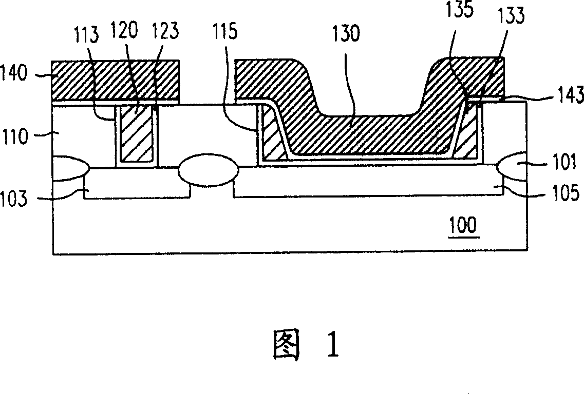
[0050] FIG. 1 is a schematic cross-sectional view of an integrated circuit structure according to an embodiment of the present invention. Referring to FIG. 1 , the integrated circuit structure includes a substrate 100 , a heavily doped region 103 , a lightly doped region 105 , a contact window 120 and a Schottky contact metal layer 130 . Wherein, the heavily doped region 103 and the lightly doped region 105 are disposed in the substrate 100 , which are separated by the isolation structure 101 , for example. The heavily doped region 103 is, for example, a doped region doped with P-type or N-type dopants. The heavily doped region 103 is, for example, the source and drain of a general logic element such as a MOS element or a memory element, and is heavily doped The impurity region 103 may be disposed in a well region (not shown). The lightly doped region 103 is different depending on the conductivity type of the substrate 100, for example, if the substrate 100 is a P-type substr...


PUM


Abstract

The IC structure comprises: a substrate formed a heavy-and light-doped area, a contact window on the heavy-doped area, and a Schottky contact metal layer on light-doped area to form a Schottky diode with the substrate, wherein the material of contact window is different from the Schottky contact metal layer.

Description

technical field [0001] The invention relates to an integrated circuit structure and a manufacturing method thereof, in particular to an integrated circuit structure including a Schottky diode and a manufacturing method thereof. Background technique [0002] A Schottky diode is a rectifying device consisting of a lightly doped semiconductor layer and a metal layer on it. As a power rectification element, Schottky diodes have been widely used in many high-speed power switches such as power supply switches, motor control drives, telecom switches, factory automation, and electronic automation. [0003] However, with the narrowing of the element line width, it is necessary to use tungsten metal with better trench filling ability to make contact windows in the back-end process of integrated circuits. Schottky diodes cannot be integrated with this tungsten metal contact process, and the Schottky diodes often have to be fabricated on another chip. In this way, design and assembly ...

Claims


Application Information

Patent Timeline
Patent Type & Authority Applications(China)
IPC IPC(8): H01L27/02H01L23/532H01L29/872H01L21/82H01L21/329H01L21/768
Inventor 郑朝华
Owner UNITED MICROELECTRONICS CORP
Why Eureka
Try Eureka