

Method for producing sheet type thermosensitive resistor
A technology of thermistor and manufacturing method, applied in resistance manufacturing, resistors, non-adjustable metal resistors, etc., can solve the problems of complex manufacturing process and high manufacturing cost, and achieve the advantages of simple manufacturing process, easy operation and shortening of manufacturing process. Effect
- Summary
- Abstract
- Description
- Claims
- Application Information
AI Technical Summary
Problems solved by technology
Method used
Image

Examples
Embodiment 1
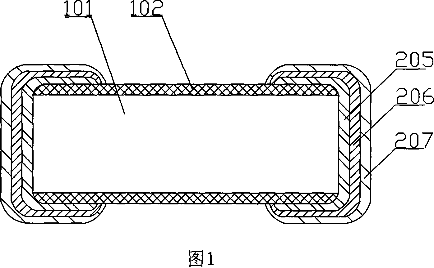
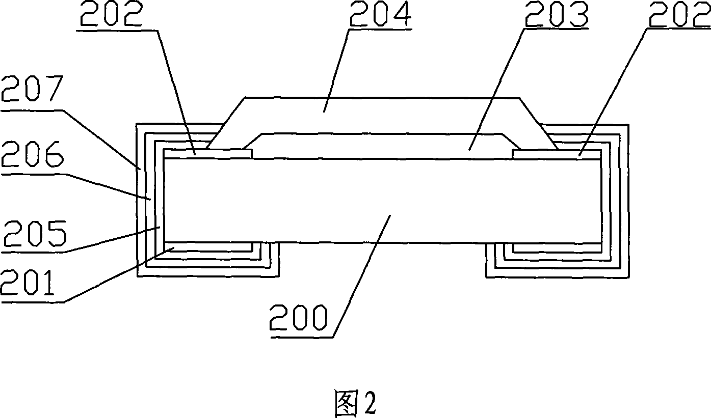
[0029] As shown in accompanying drawings 2, 4, 5, 6, 8, and 9, the chip thermistor derived by the method disclosed in the present invention includes an insulating ceramic substrate 200, a back electrode 201, a surface electrode 202, a thermistor Layer 203, protective layer 204, terminal electrode 205, intermediate electrode 206, and external electrode 207, the implementation method is as follows:
[0030] (1) On the surface of an insulating ceramic substrate 200, draw grooves vertically and horizontally according to the set intervals to form a grooved surface with a square continuous grid, and set the longitudinal groove L2, the horizontal groove L3 and the grooved surface as the front 1. The back side of the grooved surface is the reverse side; (It should be noted that the overall characteristics of the same insulating ceramic substrate are consistent, and which side is scratched is random. The setting of the grooved surface and the front and back sides here is Artificially d...
Embodiment 2
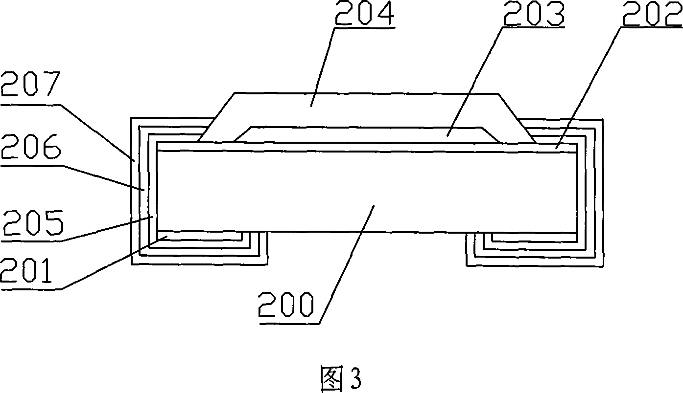
[0044] As shown in accompanying drawings 3, 4, 5, 7, 8, and 9, another chip thermistor derived from the method disclosed in the present invention includes an insulating ceramic substrate 200, a back electrode 201, a surface electrode 202, a thermistor Layer 203, protective layer 204, terminal electrode 204, intermediate electrode 206, and external electrode 207, the implementation method is as follows:
[0045] (1) On the surface of an insulating ceramic substrate 200, grooves are drawn vertically and horizontally at a set interval to form a grooved surface with a square continuous grid, and the longitudinal groove L2 and the horizontal groove L3 are set;
[0046] (2) Use the thick film screen printing method to print the conductive paste on the back of the insulating ceramic substrate 200 with each unit grid as the basis, and form the layered back electrodes 201 attached to both ends grid by grid, after conventional drying and sintering , forming a stable electrode film layer...
PUM
 Abstract
Description
Claims
Application Information