

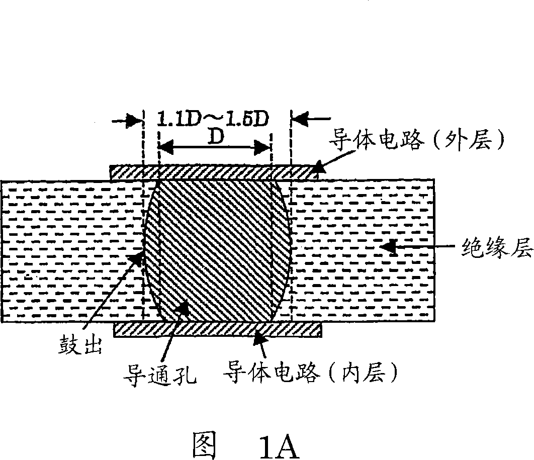
Multilayer printed wiring board
A multi-layer printing and circuit board technology, which is applied in the fields of printed circuit, printed circuit, printed circuit manufacturing, etc., can solve the problems of increasing the rigidity of the insulating substrate, reducing the rigidity of the mounting substrate, and easily reducing the resistance, so as to prevent the conductor circuit from breaking or Disconnection, reduced reliability reduction, reduced reliability reduction effect
- Summary
- Abstract
- Description
- Claims
- Application Information
AI Technical Summary
Problems solved by technology
Method used
Image

Examples
Embodiment 1
[0129] (1) First, a circuit board as a unit constituting a multilayer printed circuit board is produced. This circuit board is a substrate that is the center of lamination among a plurality of insulating layers to be laminated. A prepreg sheet that is made into a B-stage by impregnating epoxy resin on glass cloth is laminated with copper foil and heated. The double-sided copper-clad laminate 10 obtained by pressing was used as a raw material (refer FIG. 9A).
[0130] The thickness of the insulating base material 12 is 60 μm, and the thickness of the copper foil 14 is 12 μm. If a copper foil thicker than 12 μm is used as the copper foil of the laminate, the thickness of the copper foil can also be adjusted to 12 μm by etching the copper foil.
[0131] (2) Carry out carbon dioxide gas laser irradiation on the double-sided circuit board 10 that has copper foil 14, penetrate copper foil 14 and insulating base material 12, form the via hole formation opening 16 that reaches the co...
Embodiment 2
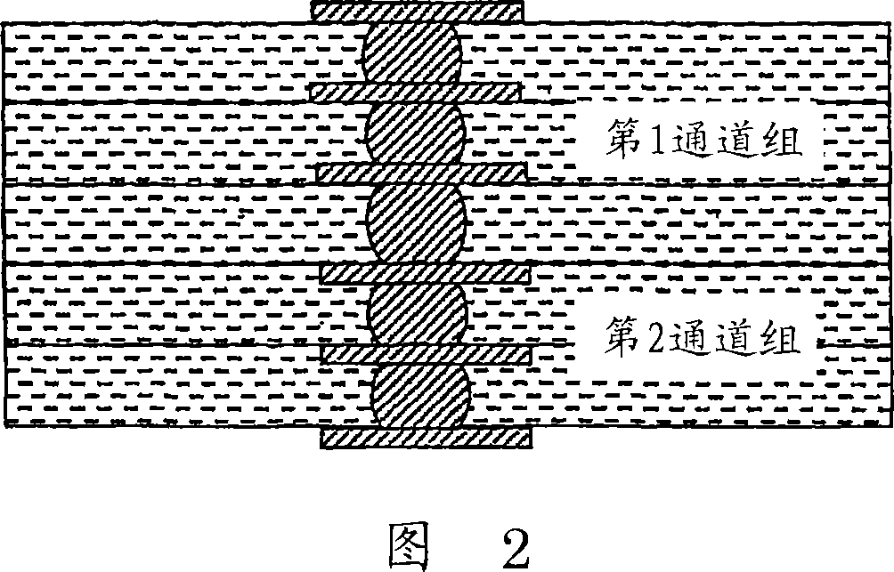
[0189] Each via hole constituting the first channel group and the second channel group formed on the insulating layer laminated on the surface and the back surface of the above-mentioned double-sided circuit board respectively, as shown in FIG. A multilayer printed wiring board was manufactured in substantially the same manner as in Example 1 except that the position was formed at a distance of about 1 / 2.
Embodiment 3
[0191] Each via hole that constitutes the first channel group formed on the above-mentioned double-sided circuit board and the insulating layer stacked above it, and the second channel group formed on the insulating layer stacked below the double-sided circuit board, as shown in the figure As shown in 3B, a multilayer printed wiring board was manufactured in substantially the same manner as in Example 1 except that the via holes were formed at positions offset from each other by about 1 / 2 of the diameter of the via holes.
PUM
| Property | Measurement | Unit |
|---|---|---|
| Thickness | aaaaa | aaaaa |
| Thickness | aaaaa | aaaaa |
| Thickness | aaaaa | aaaaa |
Abstract
Description
Claims
Application Information