Inductance coupling plasma processing device and plasma processing method

A technology of plasma and inductive coupling, applied in the direction of plasma, circuit, discharge tube, etc., can solve the problems of increased power cost, device cost, and power loss, etc., and achieve the effect of increased cost and high control accuracy

Active Publication Date: 2007-11-21
TOKYO ELECTRON LTD
View PDF2 Cites 31 Cited by
  • Summary
  • Abstract
  • Description
  • Claims
  • Application Information

AI Technical Summary

Problems solved by technology

[0008] However, in the technique described in Patent Document 1, two high-frequency power supplies or power distribution circuits, namely a high-frequency power supply for the inner part of the helical antenna and a high-frequency power supply for the outer part, need t

Method used


Image

  • Inductance coupling plasma processing device and plasma processing method
  • Inductance coupling plasma processing device and plasma processing method
  • Inductance coupling plasma processing device and plasma processing method

Examples


Embodiment Construction

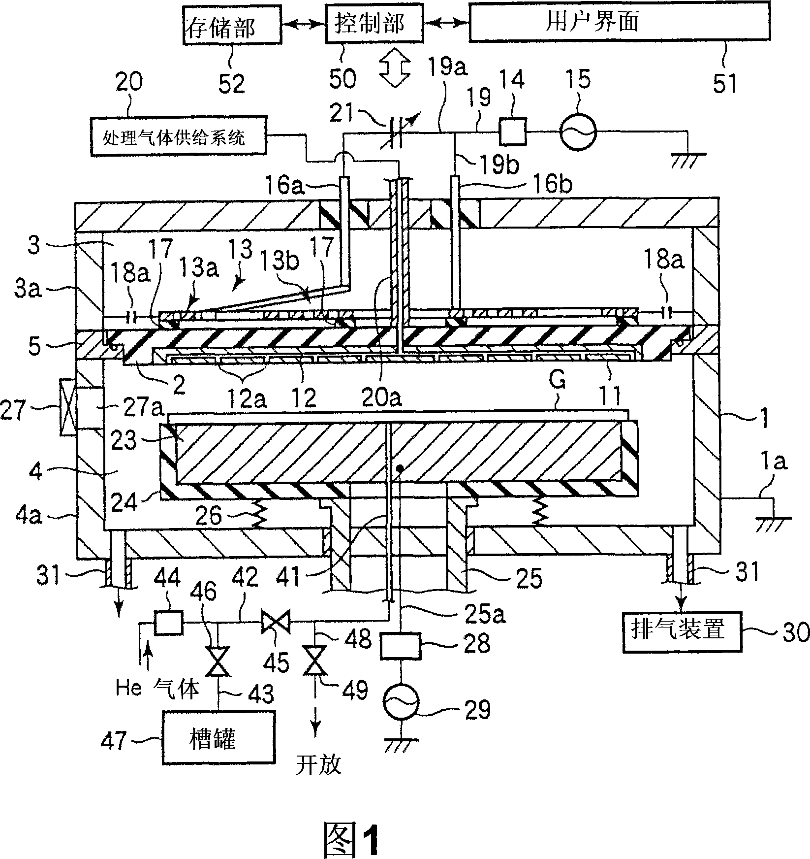
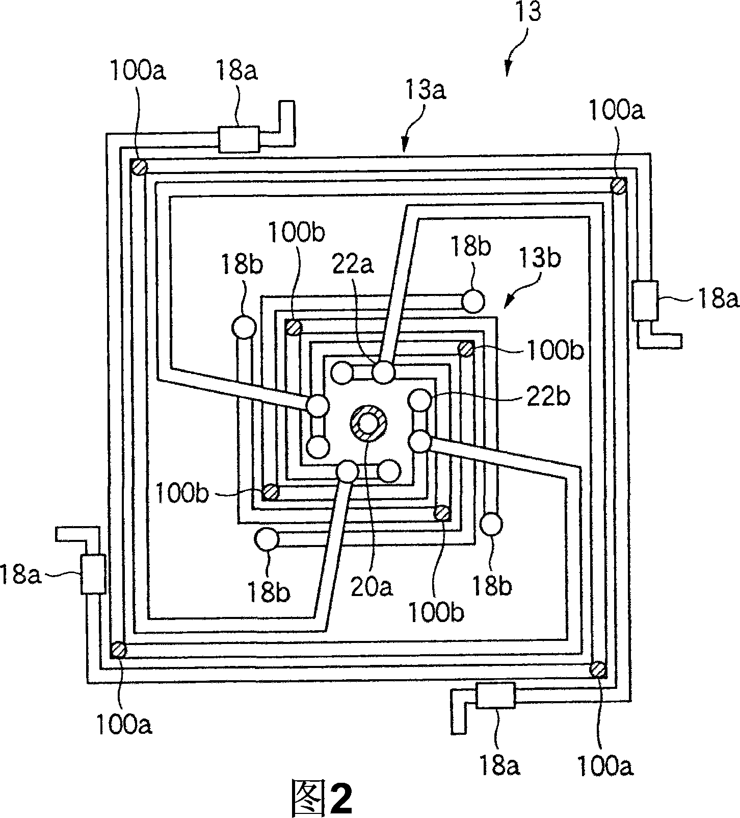
[0052] Hereinafter, embodiments of the present invention will be described with reference to the accompanying drawings. 1 is a cross-sectional view showing an inductively coupled plasma processing apparatus according to an embodiment of the present invention, and FIG. 2 is a plan view showing a high-frequency antenna used in the inductively coupled plasma processing apparatus. This apparatus can be used for, for example, etching of metal films, ITO films, oxide films, etc., and ashing of resist films when forming thin film transistors on a glass substrate for FPD. Here, the FPD includes, for example, a liquid crystal display (LCD), a light emitting diode (LED) display, an electroluminescence (Electro Luminescence: EL) display, a fluorescent display tube (Vacuum Fluorescent Display: VFD), a plasma display panel (PDP), and the like. .

[0053] This plasma processing apparatus has an airtight main body container 1 in the shape of a square cylinder made of a conductive material, ...


PUM


Abstract

The invention provides an inductance coupling plasma processing device, which can control plasma density of high precision, without replacing aerial, increasing the device price and electric power cost. A HF antenna (13) is installed by dielectric wall (2) above the processing chamber (4) and the said HF antenna comprises an outside aerial part (13a) forming induction field on the lateral part through applying the electric power of high frequency in the processing chamber (4) and inside aerial part (13b) forming induction field on the medial part and the variable capacitor (21) is connected with one side of the outside aerial part (13a) and the inside aerial part (13b). The current value of the outside aerial part (13a) and the inside aerial part (13b)is controlled through adjusting the capacitivity of the variable capacitor (21) and the plasma density distribution of the inductance coupling plasma formed in the processing chamber (4) is also controlled.

Description

technical field [0001] The present invention relates to an inductively coupled plasma processing apparatus and a plasma processing method for performing plasma processing on substrates such as glass substrates for manufacturing flat panel displays (FPD) such as liquid crystal display devices (LCD). Background technique [0002] In the manufacturing process of a liquid crystal display device (LCD) etc., in order to apply predetermined processing to a glass substrate, various plasma processing apparatuses, such as a plasma etching apparatus and a plasma CVD film-forming apparatus, can be used. Conventionally, a capacitively coupled plasma processing apparatus has been used as such a plasma processing apparatus. However, recently, an inductively coupled plasma (ICP) processing apparatus has the great advantage that high-density plasma can be obtained in a high degree of vacuum. is getting people's attention. [0003] In the case of an inductively coupled plasma processing appa...

Claims


Application Information

Patent Timeline
IPC IPC(8): H05H1/46C23C4/00C23C16/50H01L21/3065H01L21/205
CPCH01J37/321H01J37/32174H01L21/02274H01L21/3065H05H1/46
Inventor 斋藤均佐藤亮
Owner TOKYO ELECTRON LTD
Why Eureka
Try Eureka