

Near-infrared high-transmission rate and multi-crystal transparent conductive oxide film and its making method
A conductive oxide, polycrystalline transparent technology, applied in semiconductor/solid-state device manufacturing, circuits, electrical components, etc., can solve the problems of film transparency decline, conductivity limitation, etc., and achieve good application prospects, uniform film, and deposition rate high effect
- Summary
- Abstract
- Description
- Claims
- Application Information
AI Technical Summary
Problems solved by technology
Method used
Image

Examples
Embodiment 1
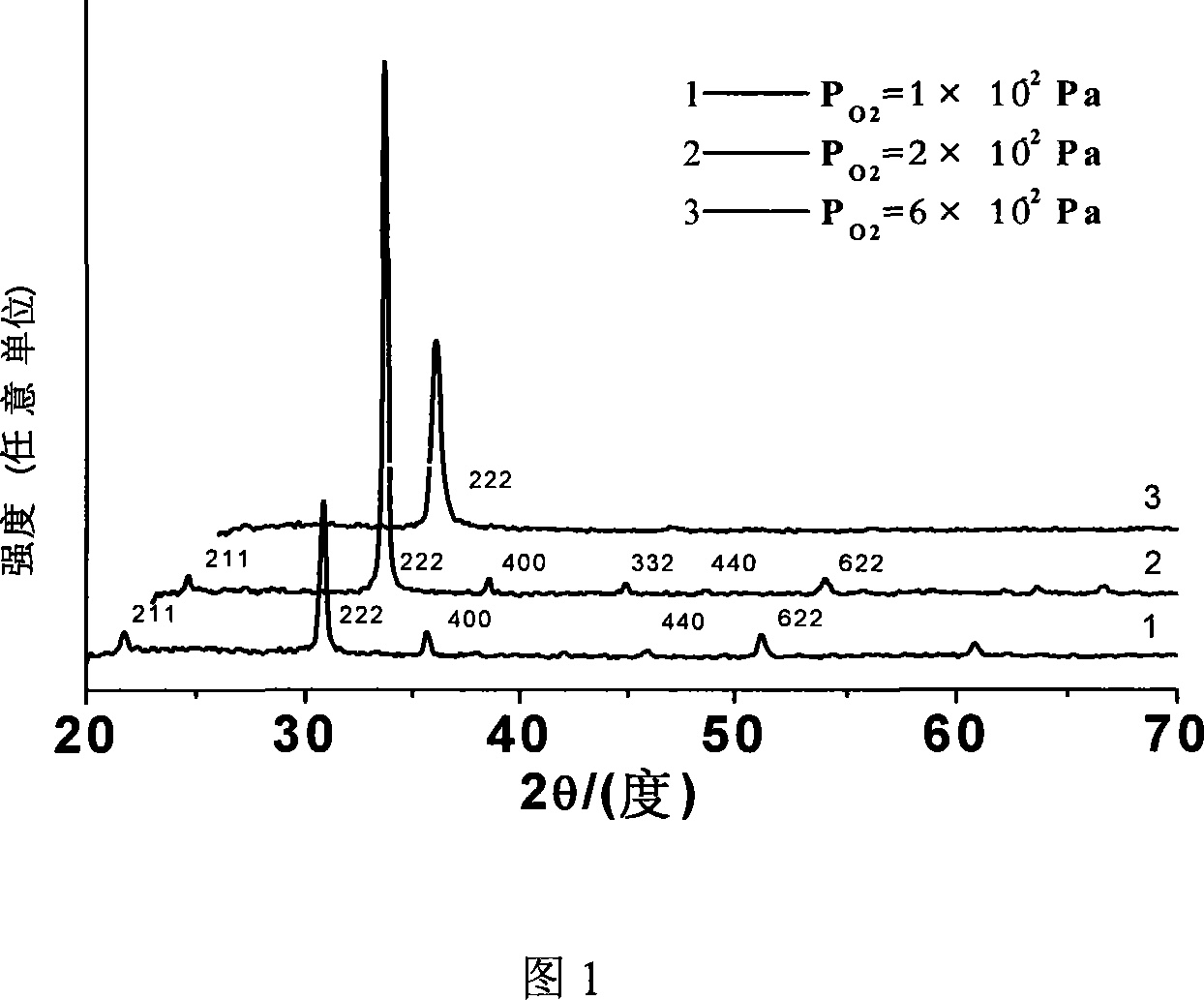
[0019] Example 1, preparation of tungsten-doped indium oxide target: In metal with a purity of 99.99% is melted into a target, and 2 wt% of tungsten wire with the same purity of 99.99% is evenly and symmetrically embedded, and the target diameter is 51mm and the thickness is 3.0mm . The substrate is a common glass slide, which has been washed by pure water, alcohol and acetone ultrasonic waves for 15 minutes each.
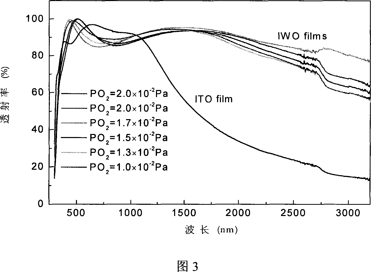
[0020] Substrate temperature: 322°C. The distance between the target and the substrate was fixed at 100 mm. Before film deposition, the reaction chamber was evacuated to less than 2×10 -3 Pa, then the O through the variable air pilot valve 2 And Ar gas into the reaction chamber. The working pressure in the reaction chamber is 3.0×10 -1 Pa, sputtering current is 100mA, sputtering voltage is 400V, control O 2 The partial pressure of the reaction gas is 2×10 -2 Pa. The film was prepared on an ordinary glass plate, the sputtering time was 10 minutes, and the fi...
Embodiment 2
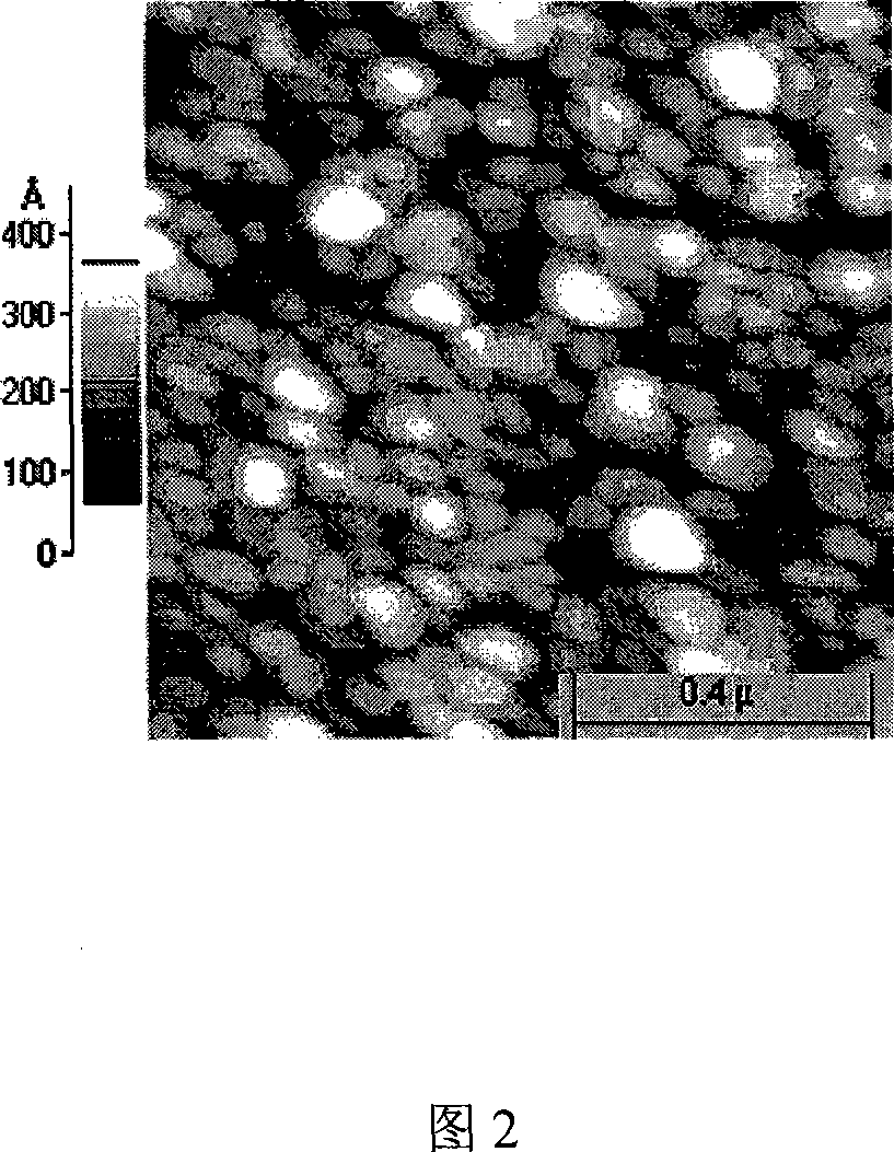
[0021] Example 2, at a substrate temperature of 315°C, the same method as in Example 1 was used to prepare a polycrystalline IWO thin film under the following conditions: the sputtering current was 100mA, the sputtering voltage was 450V, and the O 2 and Ar gas into O 2 reaction chamber and control O 2 The partial pressure of the reaction gas is 1×10 -2 Pa. The sputtering time is 10 minutes, and the film thickness is 100 nm. The resistivity of the film is 5.0×10 -4 Ω·cm, carrier mobility is 61cm 2 / V·s, the average transmittance in the visible light range is 82%, and the average transmittance in the near-infrared region is greater than 90%.
Embodiment 3
[0022] Example 3, preparation of molybdenum-doped indium oxide target: In metal with a purity of 99.99% is melted into a target, and 3 wt% of molybdenum wire with the same purity of 99.99% is uniformly and symmetrically embedded, and the target diameter is 51mm and the thickness is 3.0mm . The substrate is a common glass slide, which has been washed by pure water, alcohol and acetone ultrasonic waves for 15 minutes each.
[0023] Substrate temperature: 350°C. The distance between the target and the substrate was fixed at 95mm. Before film deposition, the reaction chamber was evacuated to less than 2×10 -3 Pa, then the O through the variable air pilot valve 2 And Ar gas into the reaction chamber. The working pressure in the reaction chamber is 1.7Pa, the sputtering current is 200mA, the sputtering voltage is 400V, and the control O 2 The partial pressure of the reaction gas is 1.5×10 -2 Pa. The film was prepared on an ordinary glass plate, the sputtering time was 10 minu...
PUM
| Property | Measurement | Unit |
|---|---|---|
| Diameter | aaaaa | aaaaa |
| Thickness | aaaaa | aaaaa |
| Thickness | aaaaa | aaaaa |
Abstract
Description
Claims
Application Information