Semiconductor package having non-ceramic based window frame

A window frame and semiconductor technology, applied in semiconductor devices, semiconductor/solid-state device components, light guides, etc., can solve problems such as interference with die installation

Inactive Publication Date: 2007-11-28
KYOCERA INT
View PDF0 Cites 8 Cited by
  • Summary
  • Abstract
  • Description
  • Claims
  • Application Information

AI Technical Summary

Problems solved by technology

However, during assembly of the header, brazing material located at the interface between the window frame and the flange may flow into the die attach area, interfering with subsequent mounting of the die in this area

Method used


Image

  • Semiconductor package having non-ceramic based window frame
  • Semiconductor package having non-ceramic based window frame
  • Semiconductor package having non-ceramic based window frame

Examples


Embodiment Construction

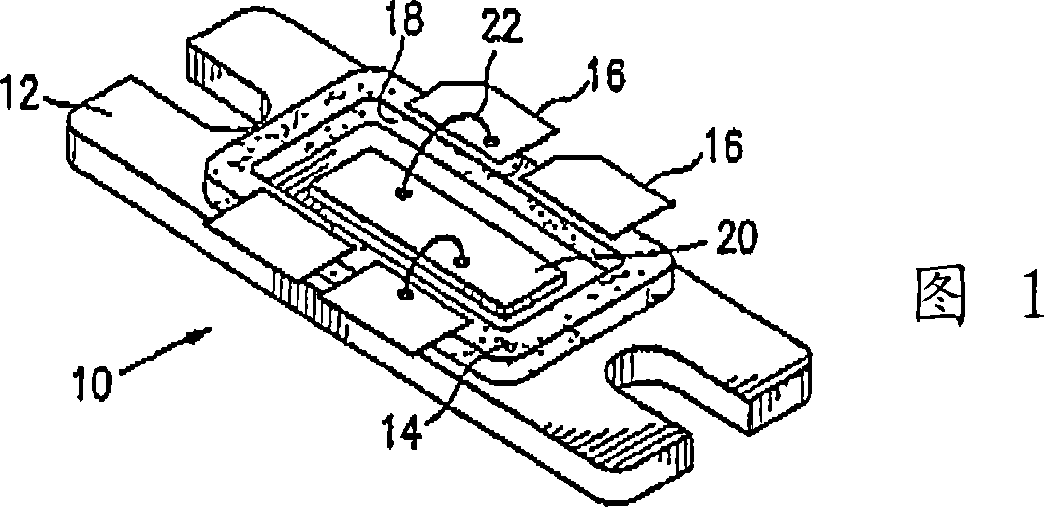
[0024] FIG. 1 shows a semiconductor package 10 according to the present invention. The package 10 in FIG. 1 includes a heat sink flange 12 of elongated, planar, generally planar configuration with a window frame 14 mounted thereon. A plurality of lead wires 16 are mounted on the window frame 14 opposite to the flange 12 . The window frame 14 has an opening 18 therein exposing a portion of the flange 12 . Semiconductor die 20 is mounted in opening 18 of flange 12 and is electrically coupled to leads 16 . Such electrical coupling may be accomplished with wire bonds 22, two of which are shown in FIG. 1 for illustration. A single die is shown in Figure 1 for illustration purposes, multiple dies may be mounted within the opening if desired. A cover (not shown) may be mounted over the leads 16 so as to extend over and surround the opening 18 and the contained die 20 .

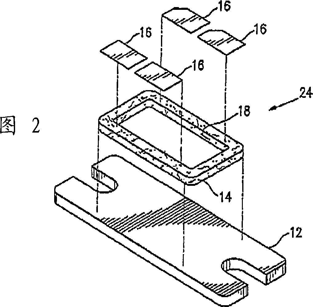
[0025] FIG. 2 is an exploded view of several components of the semiconductor package shown in FIG. 1 showing t...


PUM


Abstract

A semiconductor package for power transistors and the like has a heat sink flange with at least one die mounted thereon, a non-ceramic based window frame mounted thereon adjacent the die, and a plurality of leads mounted on the window frame and electrically coupled to the die by wire bonds. The non-ceramic based window frame is thermally matched to copper or other highly conductive material typically used for the flange, to facilitate assembly of the semiconductor package at high temperatures. The non-ceramic based window frame is flexible and is thermally matched to the highly conductive flange so as to expand and contract at a rate similar to the flange to prevent failure during assembly of the semiconductor package. The non-ceramic based material of the window frame includes a matrix of principally organic material, such as polytetrafluoroethylene, filled with fibers which may be glass fibers or ceramic fibers. The matrix is clad in a metal such as copper or aluminum, and may be coated with nickel and gold to facilitate bonding of the window frame to the flange and the leads with gold/germanium solder. The window frame may also be bonded to the flange using epoxy. Cladding of the window frame may be performed by laminating copper or other cladding metal on the matrix in a sufficient thickness so as to form the flange. The flange may be provided with a pedestal extending upwardly from an upper surface at a central portion thereof to define a die attach area and forming a barrier to brazing material used to join the window frame to the flange.

Description

technical field [0001] The present invention relates to semiconductor packages, and more particularly, to a package that mounts one or more dies on a flange located within an opening of a window frame on which the window frame is mounted, And lead wires are installed thereon. Background technique [0002] It is known in the art to provide semiconductor packages in which one or more die are mounted on a heat sink flange located within an opening of a window frame and a plurality of leads are mounted and insulated on the flange. The die may be of the LDMOS (Laterally Diffused Metal Oxide Semiconductor) type, and the package may be of the type used to package the LDMOS power transistor. A window frame, usually made of a ceramic based material such as alumina, is used to mount the leads on the semiconductor package and to insulate the leads from the heat sink flange and other package parts. The window frame has an opening therein surrounding the semiconductor die. The die is ...

Claims


Application Information

Patent Timeline
Patent Type & Authority Applications(China)
IPC IPC(8): H01J29/80H01K5/00H05K3/34H05K7/20H05K3/30H01L23/02H01L23/043G02B6/00G02B6/36H01L23/047H01L23/057H01L23/367
CPCH01L23/047H01L23/057H01L2924/01078H01L23/3675H01L2224/48137H01L2924/01079H01L24/48H01L2924/09701H01L2224/05599H01L2224/45099H01L2224/85399H01L2924/00014H01L2224/45015H01L2924/207H01L23/14H01L23/02G02B6/36H01L23/04
Inventor 杰弗里·维尼加斯保罗·加兰乔舒亚·洛布辛格琳达·卢
Owner KYOCERA INT
Why Eureka
Try Eureka