Pressure resistant layer structure having dual-medium buried layer and SOI power device using the same

A technology of power devices and dielectric buried layers, which is applied in the direction of electric solid-state devices, semiconductor devices, semiconductor/solid-state device components, etc., and can solve problems such as the withstand voltage characteristics of low-k dielectric layer SOI high-voltage devices

Inactive Publication Date: 2007-12-05
UNIV OF ELECTRONICS SCI & TECH OF CHINA
View PDF0 Cites 16 Cited by
  • Summary
  • Abstract
  • Description
  • Claims
  • Application Information

AI Technical Summary

Problems solved by technology

Literature: Luo Xiaorong et al., The withstand voltage characteristics of variable low-k dielectric layer SOI high-voltage devices, Journal of Semiconductors, 2006; 27(5): 881-85, using low-k dielectric as the buried layer to improve the buried layer electric field and device withstand voltage, However, low-k dielectric SOI has encountered challenges in being compatible with conventional CMOS processes

Method used


Image

  • Pressure resistant layer structure having dual-medium buried layer and SOI power device using the same
  • Pressure resistant layer structure having dual-medium buried layer and SOI power device using the same
  • Pressure resistant layer structure having dual-medium buried layer and SOI power device using the same

Examples


Embodiment 1

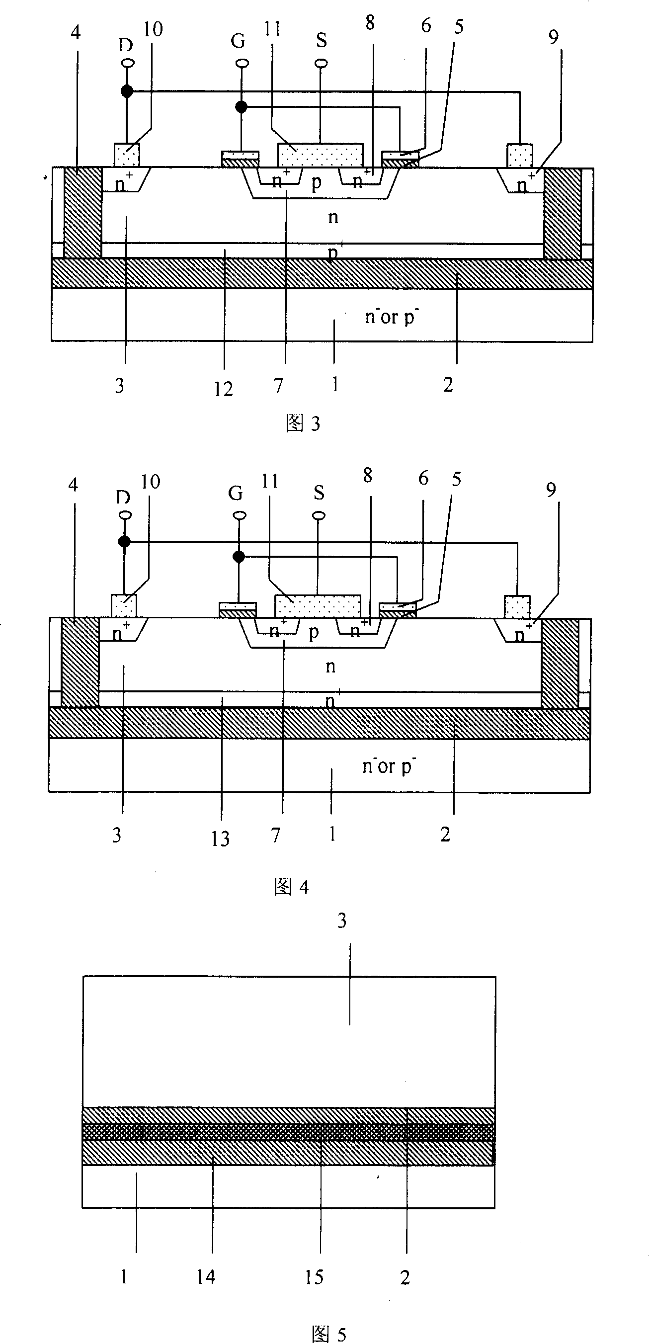
[0047] Embodiment 1: SOI structure with double dielectric buried layer

[0048] Fig. 5 is a schematic diagram of the SOI structure with double dielectric buried layers according to the present invention.

[0049] As shown in FIG. 5 , 1 is a substrate layer, 2 is a first dielectric layer (buried layer), 3 is an active semiconductor layer (S layer), 14 is a second dielectric layer (buried layer), and 15 is an intermediate layer. The intermediate layer 15 is located between the first dielectric layer (buried layer) 2 and the second dielectric layer (buried layer) 14, the other side of the first dielectric layer is connected to the active semiconductor layer 3, and the other side of the second dielectric layer 14 is connected to the The substrate layer 1 is connected.

Embodiment 2

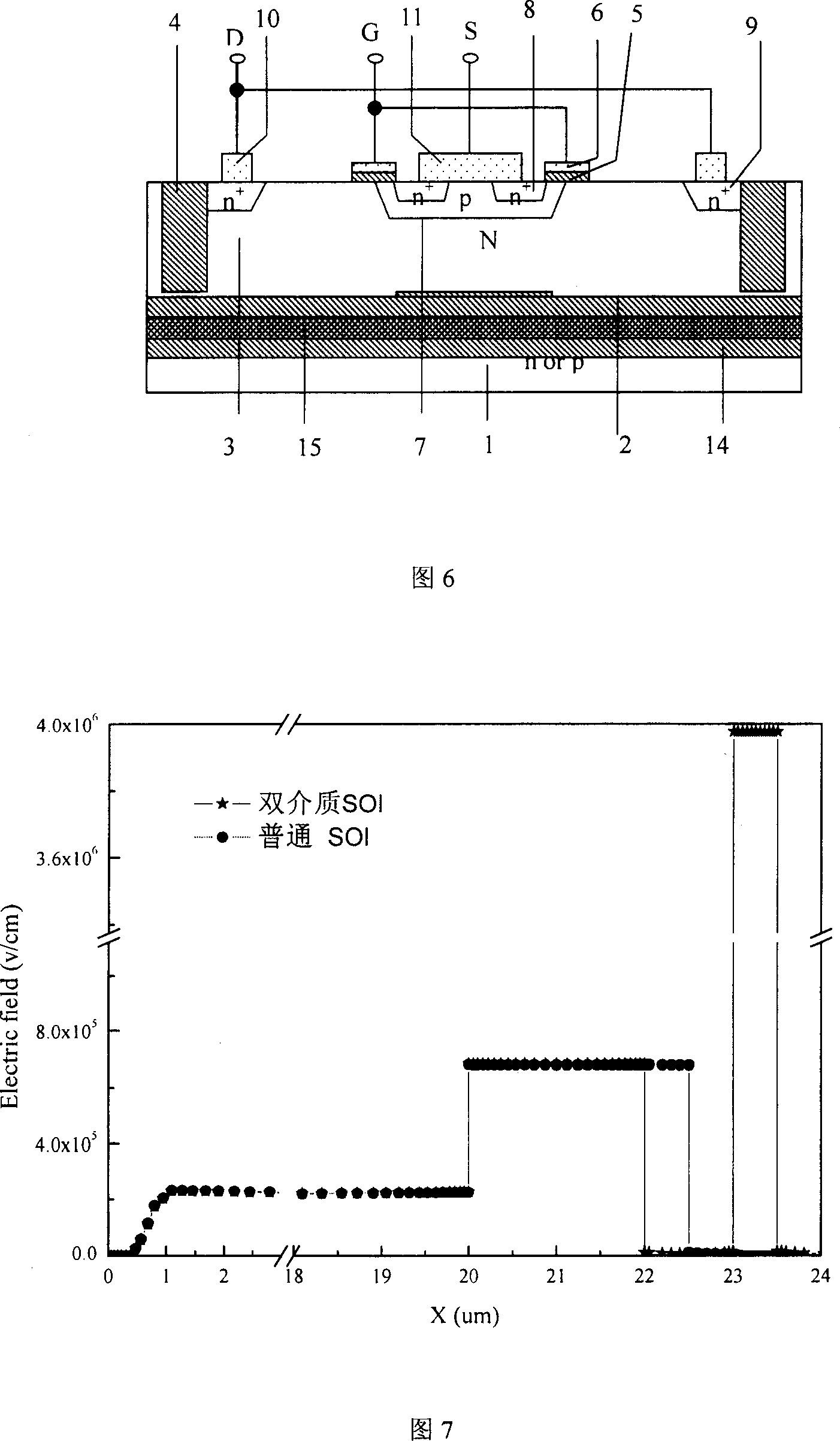
[0050] Embodiment 2: SOI LDMOS device structure with double dielectric buried layer

[0051] Fig. 6 is a schematic structural diagram of the SOI LDMOS device with double buried dielectric layers according to the present invention, and Fig. 7 is a vertical electric field distribution diagram of the 8OI LDMOS device with double buried dielectric layers according to the present invention. It can be seen that the electric field on the dielectric layer 14 is much higher than that of the conventional SOI LDMOS dielectric layer. Therefore, under the same thickness of the buried dielectric layer, the withstand voltage of the structure proposed by the present invention is greatly improved. Fig. 8a is a two-dimensional equipotential diagram of a SOI LDMOS device with a conventional structure when it breaks down. Fig. 8b is a two-dimensional equipotential diagram at the time of breakdown of the SOI LDMOS device with double dielectric buried layers according to the present invention. The...

Embodiment 3

[0053] Embodiment 3: SOI IGBT device structure with double dielectric buried layer

[0054] Fig. 9 is a schematic diagram of the SOI IGBT device structure with double dielectric buried layers according to the present invention. As shown in Figure 9, 1 is the substrate layer, 2 is the first dielectric layer, 3 is the active semiconductor layer (S layer), 6 is the gate electrode, 7 is the p (or n) well, and 8 is the n + (or p + ) cathode area, 9 is n + (or p + ) anode region, 14 is the second dielectric layer (buried layer), 15 is the intermediate layer, 17 is the anode, 18 is the cathode, and 19 is the p (or n) well. The intermediate layer 15 is located between the first dielectric layer (buried layer) 2 and the second dielectric layer (buried layer) 14, the other side of the first dielectric layer is connected to the active semiconductor layer 3, and the other side of the second dielectric layer 14 is connected to the The substrate layer 1 is connected.


PUM


Abstract

The invention provides a voltage resistance layer structure with double medium buried layers for SOI power device, and the SOI power device adopting the voltage resistance layer structure, belonging to the field of voltage resistance technique of SOI power devices. And the voltage resistance layer has double medium buried layers, where an intermediate layer is arranged between them. And the invention can improve voltage resistance on the condition of same thickness of medium buried layer, and largely reduce self-heating effect on the condition of same voltage, thus able to make a high voltage-resistance SOI power device.

Description

technical field [0001] An SOI power device with double dielectric buried layers belongs to the technical field of semiconductor power devices, and in particular relates to the technical field of voltage resistance of SOI (Semiconductor On Insulator) power devices. Background technique [0002] Power devices with SOI (Silicon on Insulator) structure (SOI power devices for short) have higher operating speed and integration, better insulation performance, stronger radiation resistance and no thyristor self-locking effect, so SOI The application of power devices in the field of VLSI has been widely concerned. The breakdown voltage of an SOI power device depends on the lower of the lateral breakdown voltage and the vertical breakdown voltage. The lateral withstand voltage design of SOI power devices follows the mature Si-based device lateral withstand voltage design principles and technologies, such as the RESURF principle and junction termination technology. However, due to th...

Claims


Application Information

Patent Timeline
Patent Type & Authority Applications(China)
IPC IPC(8): H01L29/00H01L29/786H01L29/78H01L29/739H01L29/861H01L29/74H01L27/12H01L23/00
Inventor 罗小蓉张波李肇基杨寿国詹瞻
Owner UNIV OF ELECTRONICS SCI & TECH OF CHINA
Why Eureka
Try Eureka