Semiconductor device and electronic device

A semiconductor and device technology, applied in the field of wireless communication equipment of high-frequency part analog signal processing IC, can solve the problems of reduced gain, unsatisfactory circuit components, etc., and achieve the effect of reducing crosstalk, satisfying call performance, and stable operation

Active Publication Date: 2007-12-26
RENESAS ELECTRONICS CORP
View PDF2 Cites 2 Cited by
  • Summary
  • Abstract
  • Description
  • Claims
  • Application Information

AI Technical Summary

Problems solved by technology

Therefore, in a high-speed communication system, the above-mentioned cir

Method used


Image

  • Semiconductor device and electronic device
  • Semiconductor device and electronic device
  • Semiconductor device and electronic device

Examples


Example Embodiment

[0157] (Example 2)

[0158] 14 shows a schematic plan view of a high-frequency power module of another embodiment (Embodiment 2) of the present invention when a part of the sealing body is removed.

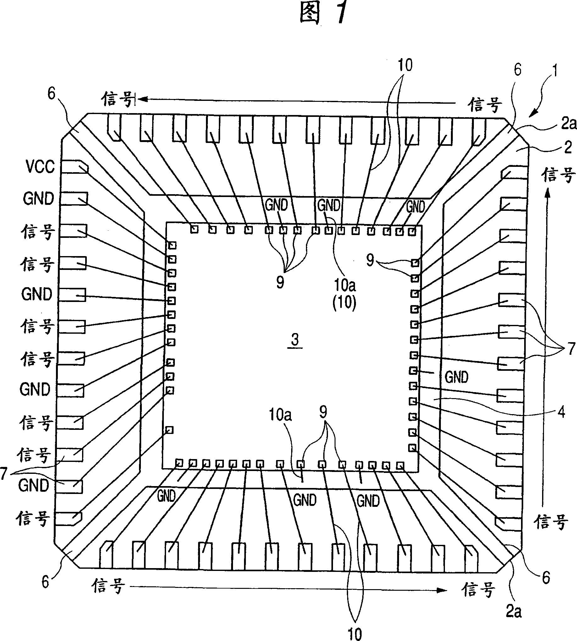
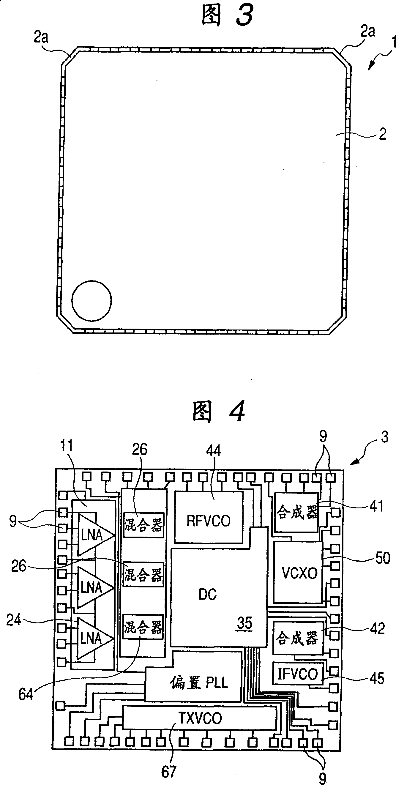
[0159] In Embodiment 1, the circuit part includes three low noise amplifiers (LNA) 24 as the designated circuit part 11 . In Embodiment 2, in addition to the above-described circuit components, in the VCO, the RFVCO 44 that handles high frequencies is used as a designated circuit component. Therefore, all the ground electrode terminals 9 of the RFVCO 44 are connected to the lead (ground lead) 7 through the wire 10, while the ground electrode terminal 9 is not connected to the tab 4 through the wire.

[0160] For the line from the electrode terminal 9 of the semiconductor chip 3 to the lead 7 through the wire 10, ground wires are provided on both sides of the two signal wires of the RFVCO 44, thus providing electromagnetic shielding for the signal wires.

[0161] Therefore, the g...

Example Embodiment

[0162] (Example 3)

[0163] 15 shows a schematic plan view of a high-frequency power module of another embodiment (Embodiment 3) of the present invention when a part of the sealing body is removed.

[0164] Embodiment 3 relates to an example in which the RFVCO 44 is provided as an external mounting member so that the semiconductor chip 3 is not formed in a monolithic circuit. In this dual-band communication method, various circuit components such as low noise amplifiers, mixers, VCOs, synthesizers, IQ modulators / demodulators, frequency dividers, DC-AC modulators, etc. are formed as monolithic circuits .

[0165] The two mixers in the receiving system are respectively controlled by a frequency divider, and the frequency divider is a frequency conversion circuit for converting a high frequency signal output from the RFVCO 44, which is an externally mounted component, into a low frequency signal.

[0166] Therefore, in Embodiment 3, as shown in FIG. 15 , the RFVCO 44 is provide...

Example Embodiment

[0168] (Example 4)

[0169] 16 and 17 relate to a high-frequency power module according to another embodiment (Embodiment 4) of the present invention, wherein FIG. 16 shows a schematic plan view of the high-frequency power module when a part of the sealing body is removed, and FIG. 17 shows the high-frequency power module. Schematic cutaway.

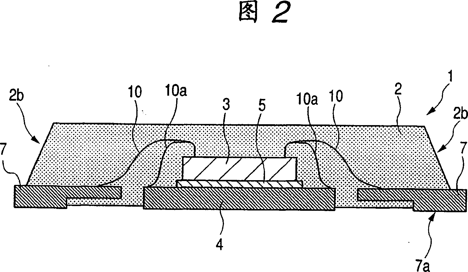
[0170] Embodiment 4 is characterized in that the tab 4 serving as a common ground terminal and the lead wire 7 taking the ground potential are electrically connected to each other using a wire 10b, and the lead wire 7 also serves as a ground external electrode terminal. In the semiconductor device 1 of Embodiment 4, since the back surface of the tab 4 is exposed from the back surface (mounting surface) of the sealing body 2, the tab 4 can be used as a ground external electrode terminal while being connected to the tab by the wire 10b The lead 7 of 4 also serves as a grounded external electrode terminal.

[0171] FIG. 18 is a modificati...


PUM


Abstract

This invention provides a high frequency power module which is incorporated into a mobile phone and which incorporates high frequency portion analogue signal processing ICs including low noise amplifiers which amplify an extremely weak signal therein. A semiconductor device includes a sealing body which is made of insulation resin, a plurality of leads which are provided inside and outside the sealing body, a tab which is provided inside the sealing body and has a semiconductor element fixing region and a wire connection region on a main surface thereof, a semiconductor element which is fixed to the semiconductor element fixing region and includes electrode terminals on an exposed main surface, conductive wires which connect electrode terminals of the semiconductor element and the leads, and conductive wires which connect electrode terminals of the semiconductor element and the wire connecting region of the tab. In such a semiconductor device, a circuit formed in the semiconductor element in a monolithic manner is comprised of a plurality of circuit parts and, in a specified circuit part (a low noise amplifier) which forms a portion of the circuit parts, all grounding electrode terminals out of electrode terminals of the semiconductor element are not connected to the tab through wires but are connected with the leads through wires.

Description

[0001] This application is a divisional application of a patent application entitled "Semiconductor Devices and Electronic Equipment" with an application date of April 28, 2003, application number 03809636.6. technical field [0002] The present invention relates to semiconductor devices and electronic equipment, and is effectively applied to, for example, high-frequency power modules (semiconductor devices), and a high-frequency part analog including a low-noise amplifier (LNA: Low Noise Amplifier) ​​for amplifying extremely weak signals The technology of the wireless communication device (electronic device) of the signal processing IC. Background technique [0003] A mobile communication device (mobile terminal) such as a mobile phone is provided to handle a plurality of communication systems. That is, in a transmission / reception unit (front end) of a mobile phone, a plurality of circuit systems are incorporated to perform transmission / reception of a plurality of communica...

Claims


Application Information

Patent Timeline
IPC IPC(8): H01L23/50H01L23/488H01L23/495H01L23/31
CPCH01L2924/01015H01L2924/01023H01L2924/01046H01L2224/4911H01L23/49503H01L2924/01082H01L2224/32245H01L2924/01002H01L24/32H01L2924/30105H01L2924/20752H01L23/50H01L2924/13091H01L2924/01019H01L2924/01029H01L2224/48091H01L2224/16245H01L2924/01087H01L2224/49171H01L2924/01013H01L2924/014H01L23/66H01L2924/30107H01L24/48H01L24/49H01L2924/01039H01L2224/92247H01L2224/45015H01L2224/484H01L24/45H01L2224/48599H01L2924/19043H01L2924/3011H01L2924/01079H01L2224/48247H01L2924/19107H01L2924/14H01L23/49548H01L2224/48011H01L2924/01033H01L2924/01005H01L2924/01006H01L23/3107H01L2924/01078H01L2924/01014H01L2224/48257H01L2224/45144H01L2224/73265H01L2924/3025H01L2924/1306H01L2924/351H01L2924/181H01L24/73H01L2224/05554H01L2224/49433H01L2924/00014H01L2924/20645H01L2924/00H01L2924/00012
Inventor 団野忠敏土屋勉
Owner RENESAS ELECTRONICS CORP
Why Eureka
Try Eureka