Low-cost and high-performance organic field effect transistor and its making method

An organic field and transistor technology, applied in the field of organic field effect transistors, can solve the problems of high cost and achieve the effect of low cost, simple process and cost reduction

Inactive Publication Date: 2008-01-09
INST OF CHEM CHINESE ACAD OF SCI
View PDF0 Cites 13 Cited by
  • Summary
  • Abstract
  • Description
  • Claims
  • Application Information

AI Technical Summary

Problems solved by technology

Ioannis Kymissis and David J. Gundlach used hexadecyl mercaptan and 4-nitrobenzene thiol to modify gold electrodes respectively to obtain high-performance organic field-effect transistors with lower electrode structure, (1: Kymissis, I.; D...

Method used


Image

  • Low-cost and high-performance organic field effect transistor and its making method
  • Low-cost and high-performance organic field effect transistor and its making method
  • Low-cost and high-performance organic field effect transistor and its making method

Examples


preparation example Construction

[0037] The preparation method of described organic field effect transistor comprises the following steps:

[0038] The first step, the deposition preparation of the source and drain electrodes

[0039] The substrate deposited with the gate electrode and insulating layer was ultrasonically cleaned with deionized water, ethanol, and acetone, and then oven-dried, then modified with octadecylchlorosilane (OTS), and then ultrasonically cleaned with n-heptane, ethanol, and acetone. Cleaned and then evaporated to deposit at least one layer of metal.

[0040] The second step, the modification of the source and drain electrodes

[0041]Drop the acetonitrile solution (5mM) of 7,7,8,8-tetracyanoquinodimethane (TCNQ) on the substrate on which the electrode is deposited, then quickly dry it, and then rinse with acetonitrile to obtain a modified organic charge Transfer the source-drain electrodes of the complex salt layer.

[0042] The third step, deposition of organic semiconductor mate...

Embodiment 1

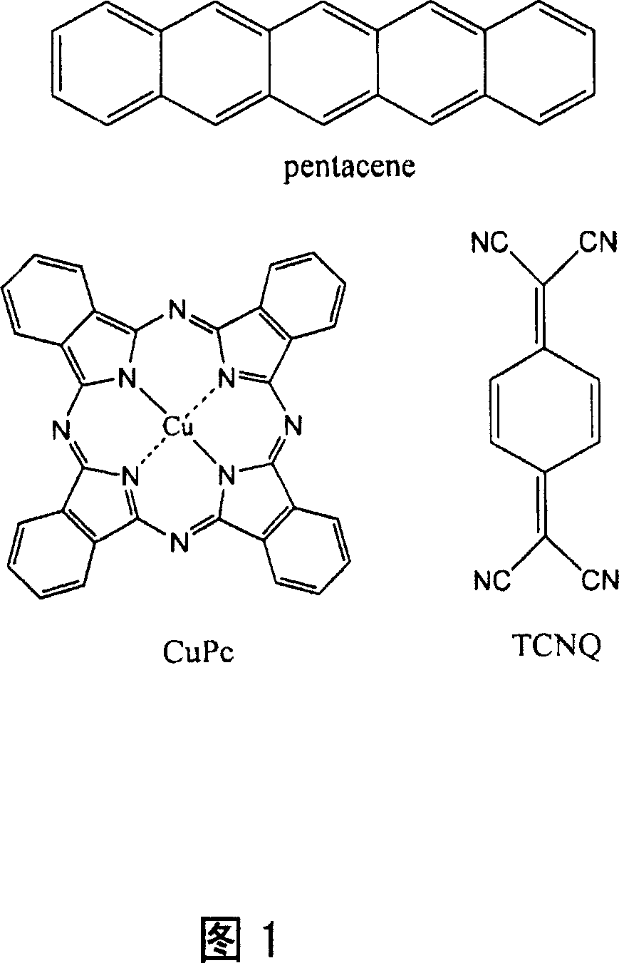
[0048] Figure 1 shows the molecular formulas of the organic materials used to prepare the present invention, which are pentacene (pentacene), copper phthalocyanine (CuPc) and 7,7,8,8-tetracyanoquinodimethane (TCNQ).

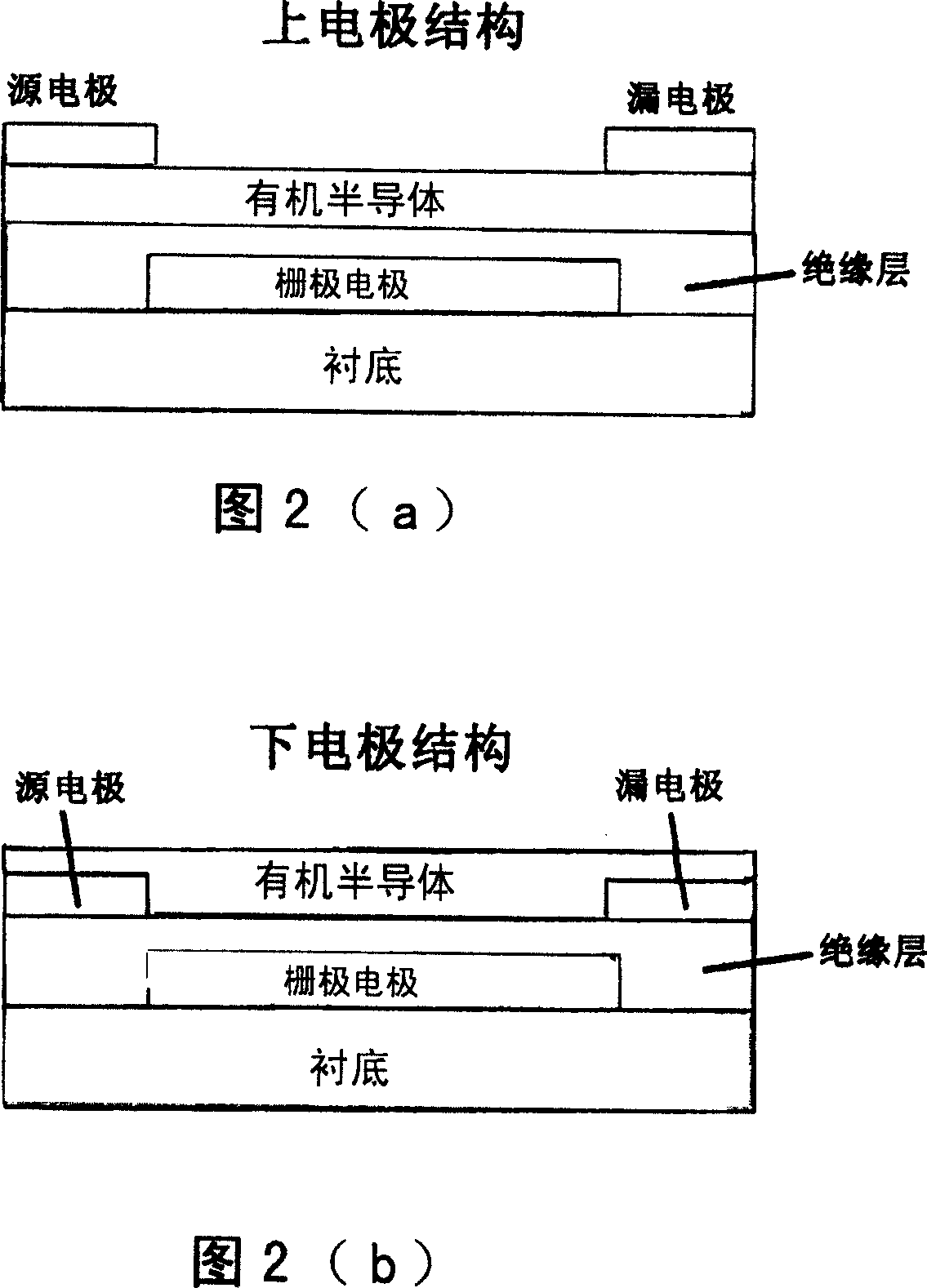
[0049] Fig. 2 schematic diagram of upper electrode structure and lower electrode structure of organic field effect transistor;

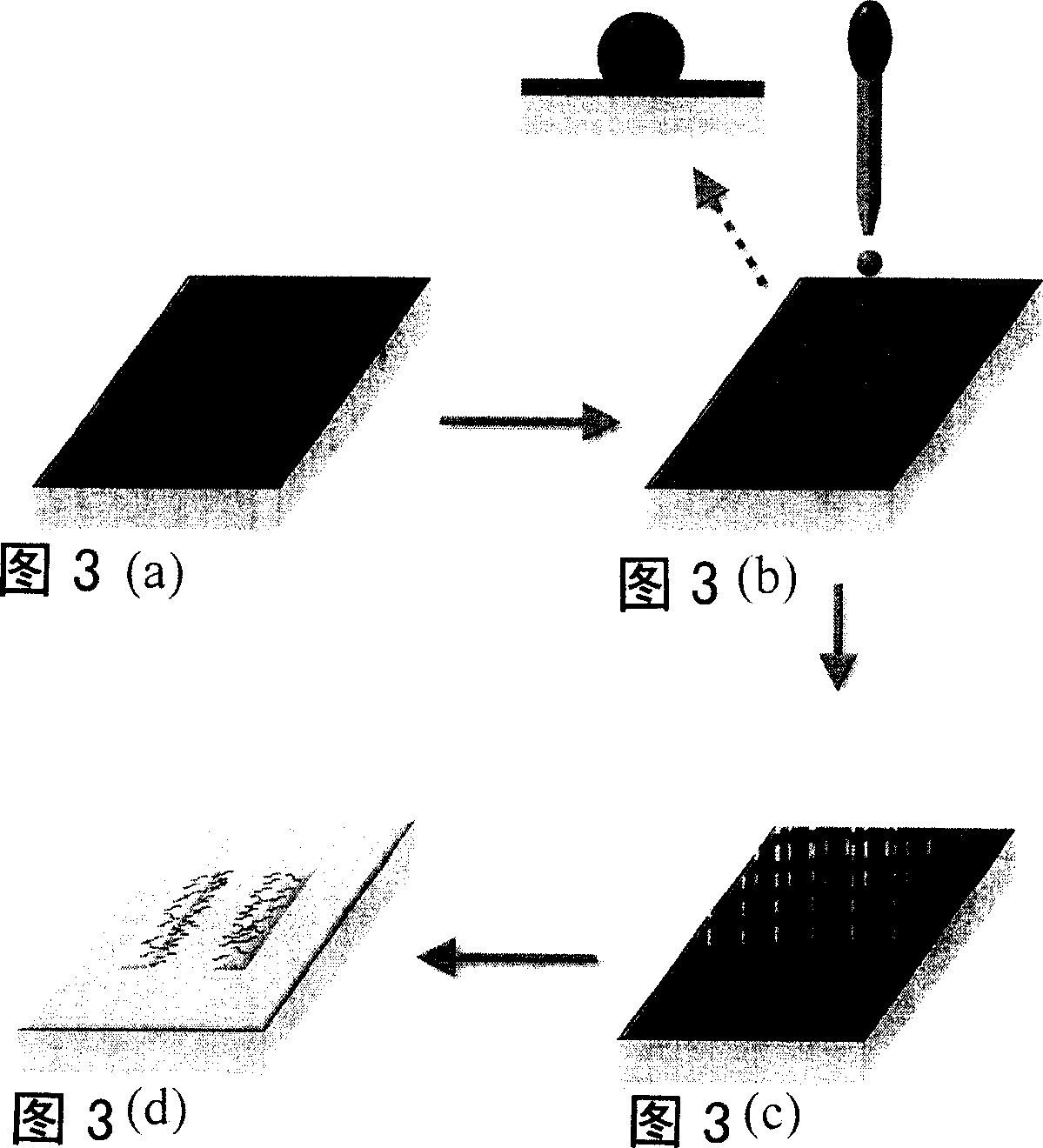
[0050] What Fig. 3 shows is the preparation flow chart of bottom electrode structure organic field effect transistor of the present invention; Wherein, Fig. 3 (a) is to depositing source-drain electrode on the substrate of silicon dioxide modified through octadecyl chlorosilane , Fig. 3(b) is to drop the acetonitrile solution of TCNQ on the substrate of prepared source-drain electrode, Fig. 3(c) is to deposit organic semiconductor on the substrate of modified electrode, Fig. 3(d) is prepared Schematic diagram of an organic field effect device.

[0051] Figure 4 is a scanning electron microscope image of the prepared device, wherein Fig...

Embodiment 2

[0065] According to the preparation of Example 1, the only difference is that Cu-TCNQ is used as the source-drain electrode, and the field-effect mobility based on pentacene is 0.056cm 2 V -1 the s -1 , an on-off ratio of 10 6 .

[0066] Referring to Fig. 6, it is the output curve and transfer curve diagram of the organic field effect transistor with Cu-TCNQ as the source and drain electrodes, and pentacene as the organic semiconductor, wherein, the output curve of Fig. 6 (a), Fig. 6 (b) It is the transfer curve when the source-drain voltage is -60V.


PUM

PropertyMeasurementUnit
Thicknessaaaaaaaaaa
Thicknessaaaaaaaaaa

Abstract

The invention is concerned with the low cost high efficient organic field effect transistor and it's making method, which belongs to the organic field effect transistor technique, with the source-drain electrode structure made from low work content material such as silver or copper, that forms the organic charge transfer complex salt layer on the surface of the organic semiconductor and the source-drain electrode. The making method includes: disposing the grid electrode and the isolating layer, and disposing the source-drain electrode on the isolating layer; decorating the source-drain electrode to cover the surface with the organic charge transfer complex salt layer; the last, disposing the organic semiconductor material on the complex salt layer. The invention insures the connection between the under metal electrode and the semiconductor for the efficient charge carrier injection.

Description

technical field [0001] The invention relates to the technical field of organic field effect transistors, in particular to a method for preparing a novel low-cost high-performance organic field effect transistor, which is an organic field effect transistor using low-cost metals as electrodes. Background technique [0002] Since the invention of organic field effect transistors (Tsumura, A.; Koezuka, H.; Ando, ​​T.Appl.Phys.Lett.1986, 49, 1210) in the 1980s, organic field effect transistors have been organically integrated in flexible displays. The potential application prospects in circuits and other aspects have aroused people's extensive research interest. Compared with inorganic transistors, organic field effect transistors have the advantages of simple preparation process, low cost, light weight, and good flexibility. In recent years, organic field effect transistors have made great progress in design and synthesis of new stable organic semiconductor materials and device...

Claims


Application Information

Patent Timeline
IPC IPC(8): H01L51/05H01L51/40
Inventor 于贵狄重安徐新军刘云圻孙艳明王鹰朱道本
Owner INST OF CHEM CHINESE ACAD OF SCI
Why Eureka
Try Eureka