Method for encapsulating LED with rotary glue and optical etching technology

A technology of light-emitting diodes and photolithography technology, which is applied in the direction of electrical components, circuits, semiconductor devices, etc., and can solve problems such as low production efficiency, application restrictions, and difficulty in ensuring seamless bonding

Active Publication Date: 2008-02-13
GUANGDONG REAL FAITH LIGHTING TECH
View PDF0 Cites 11 Cited by
  • Summary
  • Abstract
  • Description
  • Claims
  • Application Information

AI Technical Summary

Problems solved by technology

However, this method also cannot ensure that the side of the chip is evenly coated with phosphor; because it is difficult to ensure seamless bonding between the light-emitting chip and the film, the light is reflected and refracted multiple times on the interface that is not completely bonded, resulting in Decrease in light extraction efficiency; in addition, since each light-emitting chip has to be pasted with cured film, the production efficiency is very low, which is not conducive to large-scale production, and this packaging method is only suitable for flip chips, and its application is greatly restricted
As for LED chip array packaging that needs to increase luminous flux, the existing packaging methods have low production efficiency, are not conducive to large-scale production, and product performance is greatly affected by the process, and the reliability is poor.

Method used


Image

  • Method for encapsulating LED with rotary glue and optical etching technology
  • Method for encapsulating LED with rotary glue and optical etching technology

Examples


Embodiment 1

[0010] Embodiments of the present invention are further described below in conjunction with the accompanying drawings:

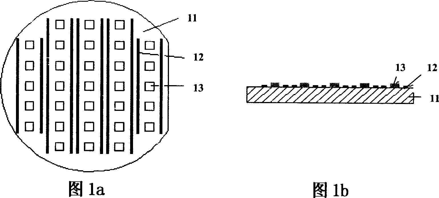
[0011] Referring to Fig. 1a and Fig. 1b, GaN blue light-emitting chips 13 and electrodes 12 are fabricated into an array on the chip substrate 11 by multi-layer epitaxy and photolithography and etching processes;

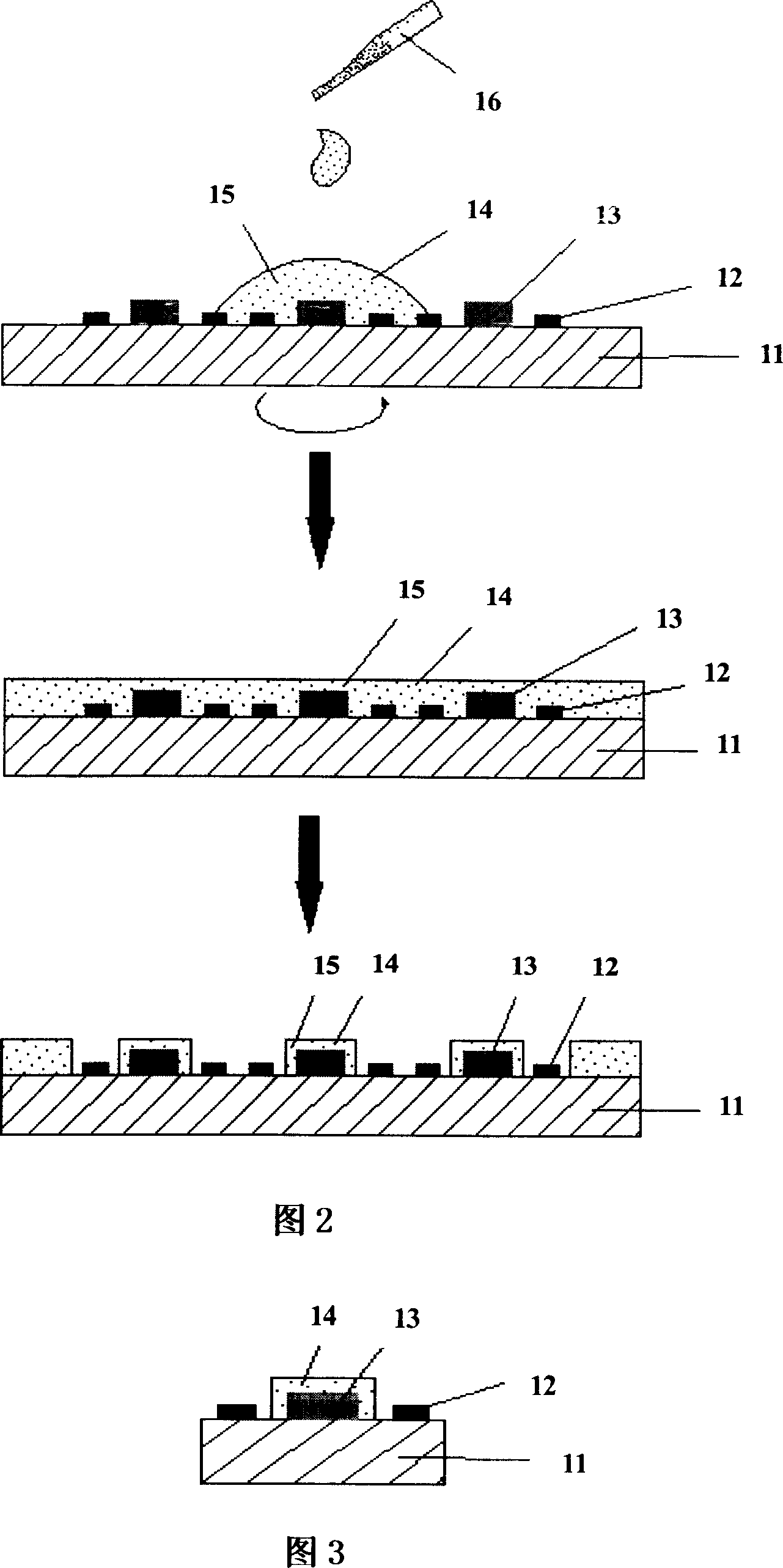
[0012] The present invention adopts glue-spinning and photolithography technology, and the glue-spinning process refers to dripping glue 14 containing fluorescent powder when the chip substrate 11 is rotating, so that the glue is evenly dispersed and coated on the chip substrate 11, and the blue-ray chip array containing GaN 13, a phosphor-containing adhesive layer 14 with a uniform thickness is formed on the surface of the chip substrate 11, and a white LED package is realized by photolithography, development, curing, and cutting processes. Referring to Fig. 2, its specific process steps are as follows:

[0013] 1) In the photolithography room, ...


PUM


Abstract

A packaging method of white LED by rotating glue and lithography process mainly comprises a monochromatic LED chip, a lead wire, a phosphor glue layer and a chip substrate. The invention is characterized in that the phosphor glue layer is fabricated by the rotating glue process for forming the phosphor glue layer on the surface of the chip substrate, then the packaging of white LED is completed by lithography, developing, solidification and cutting processes. The invention has the advantages that the packaging method of LED by the rotating glue and lithography process can accurately control the thickness of the phosphor glue layer on the chip surface, promote the light quality and uniformity of luminescence from white LED after packaging, and promote the production efficiency of packaging.

Description

technical field [0001] The invention relates to a method for manufacturing a semiconductor device, in particular to a method for encapsulating a light-emitting diode by using spinning glue and photolithography technology. technical background [0002] The existing high-brightness white light-emitting diode LED is formed by mixing various colors of light. For example, red, green and blue chips are combined to form white light through optical lens, or purple or ultraviolet light is used to excite RGB (red, green and blue) phosphors to obtain white light, or blue light is used to excite yellow phosphors to obtain white light. Among them, the use of blue LED chips to excite YAG yellow phosphors to produce white light is the most widely used. YAG yellow phosphors are mixed into epoxy resin or silica gel, mixed evenly, and then coated on blue chips by coating or dispensing. The disadvantage of this method is that if the coating dose of the yellow phosphor is not accurately contro...

Claims


Application Information

Patent Timeline
Patent Type & Authority Applications(China)
IPC IPC(8): H01L33/00H01L21/50H01L21/56H01L33/48H01L33/50
Inventor 刘胜陈明祥罗小兵甘志银
Owner GUANGDONG REAL FAITH LIGHTING TECH
Why Eureka
Try Eureka