Plasma flat panel display driving chip structure and method for preparing the same

A flat-panel display and driver chip technology, applied in semiconductor/solid-state device manufacturing, transistors, electrical components, etc., can solve the problems of large isolation structure area, withstand voltage and isolation structure limitations, insufficient domestic manufacturing capacity, etc., and achieve anti-latch-up The effect of good performance and high reliability

Inactive Publication Date: 2008-02-27
SOUTHEAST UNIV
View PDF0 Cites 8 Cited by
  • Summary
  • Abstract
  • Description
  • Claims
  • Application Information

AI Technical Summary

Problems solved by technology

The third process is limited by the withstand voltage of the device itself and the isolation structure, so it is not suitable for the up-scan driver chip above 100V.
Although the first two processes are suitable for row scanning driver chips and column addressing driver chips, both processes also have their own shortcomings: the isolation structure area of ​​the epitaxial process structure is too large, and the area of ​​the chip used for isolation exceeds 20%; SOI process structure, although the isolation area is small, less than 5% of the chip area, but the cost of SOI materials (over 7um epitaxy) that meets the requirements will be several times that of epitaxy materials, and domestic manufacturing capacity is seriously insufficient

Method used


Image

  • Plasma flat panel display driving chip structure and method for preparing the same

Examples


Embodiment 1

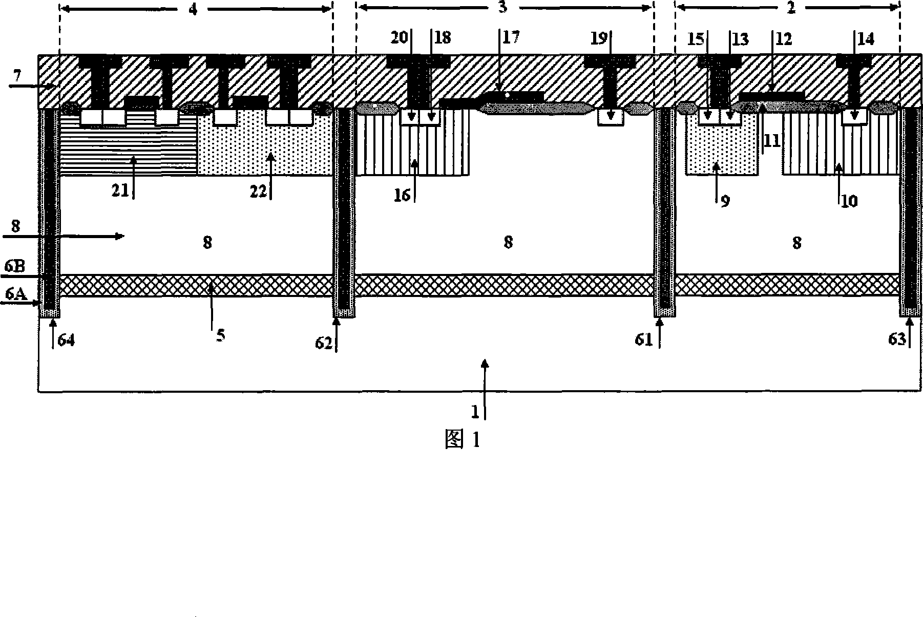
[0020] Below in conjunction with accompanying drawing, the present invention is described in detail, as shown in Figure 1, a kind of plasma panel display driver chip structure comprises P-type substrate 1, is provided with N-type epitaxial layer 8 on P-type substrate 1, in N A high-voltage-P-type lateral metal-oxide-semiconductor transistor 2, a high-voltage-N-type lateral metal-oxide-semiconductor transistor 3, and a low-voltage-complementary lateral metal-oxide-semiconductor transistor 4 are arranged on the epitaxial layer 8, and the P-type substrate 1 and the An N-type heavily doped buried layer 5 is provided between the N-type epitaxial layers 8, and the high-voltage-P-type lateral metal oxide semiconductor transistor 2, the high-voltage-N-type lateral metal-oxide semiconductor transistor 3 and the low-voltage-complementary lateral metal oxide semiconductor transistor The semiconductor transistor 4 is located above the N-type heavily doped buried layer 5, and a first trench...

Embodiment 2

[0026] The preparation method of plasma flat panel display drive chip structure of the present invention is:

[0027] The first step: take the P-type substrate 1 and pre-clean it; prepare an N-type heavily doped buried layer 5 on the P-type substrate; then grow an N-type epitaxial layer 8; carve a deep isolation groove on the epitaxial layer and Prepare silicon dioxide and fill polysilicon or silicon dioxide, separate the N-type epitaxial layer 8 to form a first N-type epitaxial region, a second N-type epitaxial region, and a third N-type epitaxial region; prepare on the first N-type epitaxial region The P-type drift region of the high-voltage P-type lateral MOS transistor, and then prepare the P-type well of the high-voltage N-type lateral MOS transistor on the second N-type epitaxial region, and prepare the N of the high-voltage P-type lateral MOS transistor on the first N-type epitaxial region. While preparing the N-type well of the low-voltage P-type MOS transistor and the...


PUM


Abstract

The present invention discloses a driving chip structure of plasma plate display and its processing method, and is applied to column-location-selection driving chip and line-scanning driving chip of the plasma plate display. The chip structure includes P-type substrate, N-type epitaxial layer set on the P-type substrate, high-pressure-P-type, high-pressure-N-type and low-pressure-complementary-type lateral MOS transistors set on the N-type epitaxial layer, N-type-heavy-doped-buried-layer-and-high-pressure-P-type lateral MOS transistor set between the P-type substrate and the N-type epitaxial layer. The high-pressure-N-type and low-pressure-complementary-type lateral MOS transistors are set above the N-type-heavy-doped buried layer. The structure and its processing method of the present invention are based on epitaxial material, and there is a big cost advantage comparing with it of using SOI.

Description

technical field [0001] The invention relates to a plasma flat panel display (PDP) drive chip structure and a preparation method thereof, which are suitable for a column address selection drive chip of a plasma flat panel display and a row scanning drive chip of a plasma flat panel display. Background technique [0002] The plasma flat panel display driver chip is controlled by low-voltage logic to realize high-voltage output. With the continuous improvement of display technology and driving technology, the plasma flat panel display driver chip has the following development trends: the operating frequency of the column address selection driver chip is continuously improved, and the integration level is continuously improved; is also continuously increasing. Currently commonly used plasma flat panel display drive chip structures and preparation methods include: (1) epitaxial process structure, integrating high-voltage nVDMOS, high-voltage pLDMOS and low-voltage CMOS, using de...

Claims


Application Information

Patent Timeline
Patent Type & Authority Applications(China)
IPC IPC(8): H01L27/092H01L21/8238H01L21/762
Inventor 李海松吴虹孙伟锋易扬波时龙兴
Owner SOUTHEAST UNIV
Why Eureka
Try Eureka