

Method for preparing p-type copper-sulfur-containing transparent conductor film
A technology of transparent conductive film and copper-sulfur, which is applied in vacuum evaporation plating, coating, sputtering plating, etc., can solve the problems that the research on sulfide film deposition has not been reported.
- Summary
- Abstract
- Description
- Claims
- Application Information
AI Technical Summary
Problems solved by technology
Method used
Image

Examples
Embodiment 1
[0028] CuAlS obtained by vacuum solid-state reaction and SPS sintering 2 The circular block is the target material, and the diameter of the target material is 15mm. The quartz glass plate was used as the substrate (substrate), and was ultrasonically cleaned by deionized water, dilute HCL, acetone, absolute ethanol, and deionized water for 20 minutes each. The distance between the fixed target surface and the substrate surface is about 5cm.
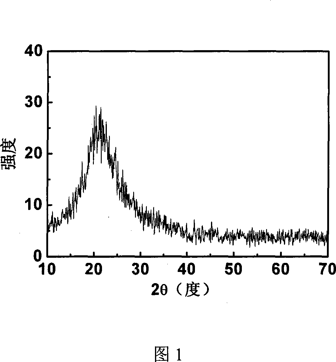
[0029] maintain a high vacuum (10 -4 Pa), the substrate temperature is controlled at 600°C, the laser energy is 120mJ, the initial frequency is 1Hz, the pre-deposition is 5min, the frequency is changed to 5Hz, the deposition time is 60min, the deposition is completed, and the temperature is lowered to room temperature, then taken out, that is Amorphous CuAlS 2 thin film (XRD see Figure 1). The thickness of the film is not very uniform, the edge is thin and the middle is thick, and the scanning electron microscope observation is between...
Embodiment 2
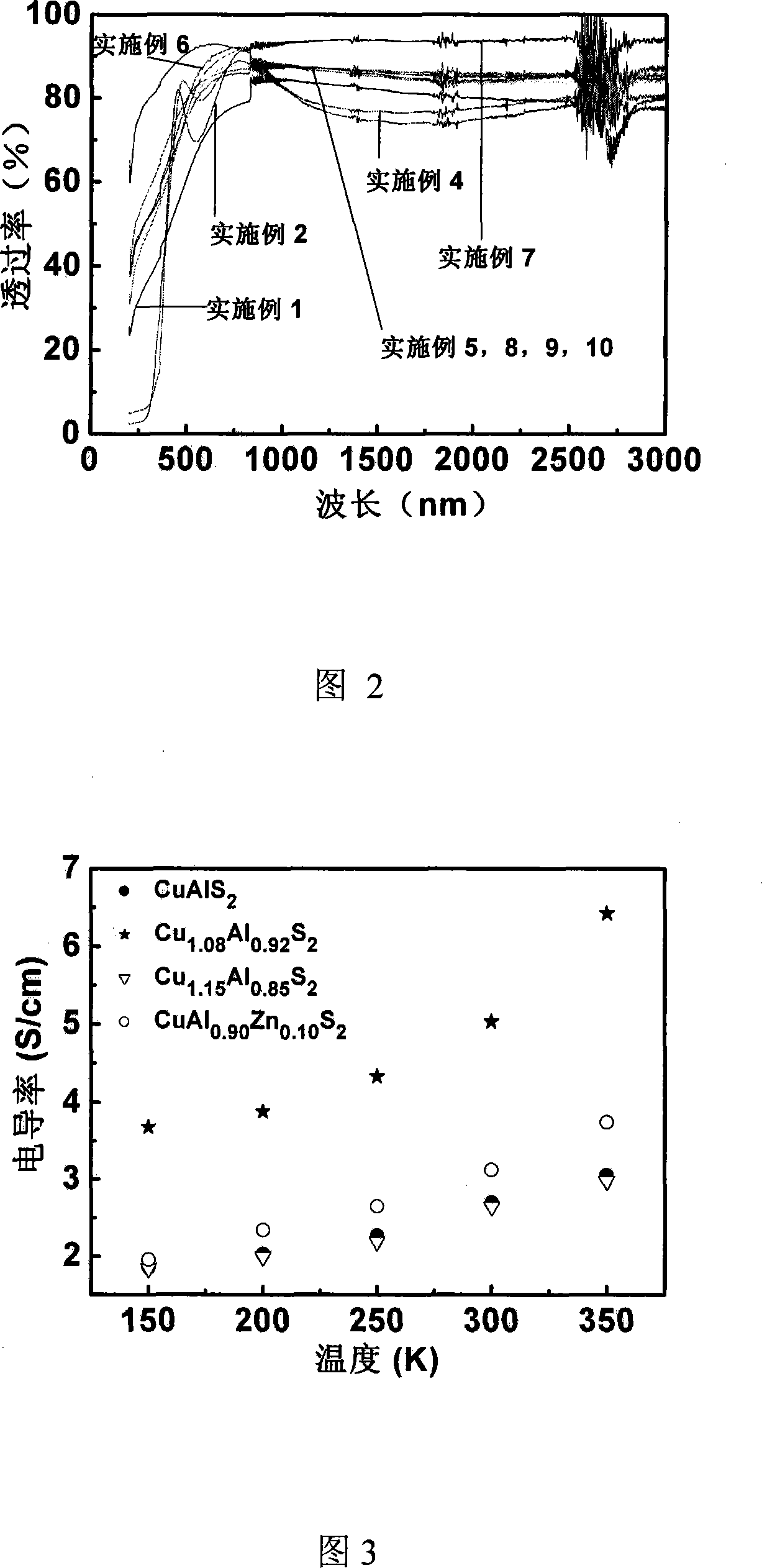
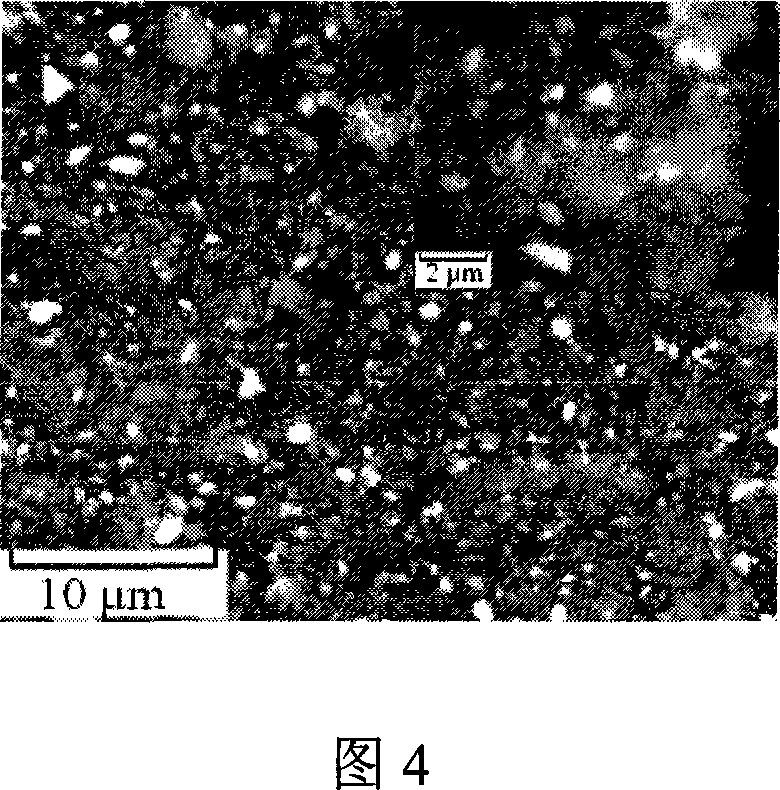
[0031] Similar to Example 1, the difference is that Ar is used as the working atmosphere, and the working pressure is 10Pa, and the obtained amorphous CuAlS 2 (XRD is similar to Example 1) The film thickness is uniform, the thickness is 100nm, and the ultraviolet-near infrared transmission spectrum (Fig. 2) shows that the average transmission rate in the visible light range is greater than 75%. The conductivity test shows that it has p-type conductivity (the Seebeck coefficient in Table 1 is positive), the conductivity at variable temperature (150K-350K) is shown in Figure 3, and the conductivity at room temperature is about 2S / cm (see Table 1).
Embodiment 3
[0033] Similar to Example 2, the only difference is that Si sheet is used as the substrate to obtain amorphous CuAlS 2 Thin film (XRD is similar to embodiment 1), film thickness is about 100nm, and the room temperature conductivity recorded is close to embodiment 2 (seeing table 1), and conductivity test shows that it has p-type conductivity (seebeck coefficient in table 1 is positive value).
PUM
| Property | Measurement | Unit |
|---|---|---|
| Conductivity at room temperature | aaaaa | aaaaa |
| Thickness | aaaaa | aaaaa |
| Conductivity at room temperature | aaaaa | aaaaa |
Abstract
Description
Claims
Application Information