Method for improving silicate nickel layer performance and method for forming PMOS transistor

A nickel silicide layer, transistor technology, applied in semiconductor devices, semiconductor/solid-state device manufacturing, electrical components, etc., can solve problems such as spike phenomenon

Inactive Publication Date: 2008-03-05
SEMICON MFG INT (SHANGHAI) CORP
View PDF1 Cites 5 Cited by
  • Summary
  • Abstract
  • Description
  • Claims
  • Application Information

AI Technical Summary

Problems solved by technology

[0011] However, the formation of the nickel silicide layer also has disadvantages in the process of manufacturing the PMOS transistor, that is, when there is tensile stress in the silicon substrate, nickel disilicide will be generated while the nickel silicide layer is formed, resulting in a spike phenomenon, which in turn leads to leakage current

Method used


Image

  • Method for improving silicate nickel layer performance and method for forming PMOS transistor
  • Method for improving silicate nickel layer performance and method for forming PMOS transistor
  • Method for improving silicate nickel layer performance and method for forming PMOS transistor

Examples


Embodiment Construction

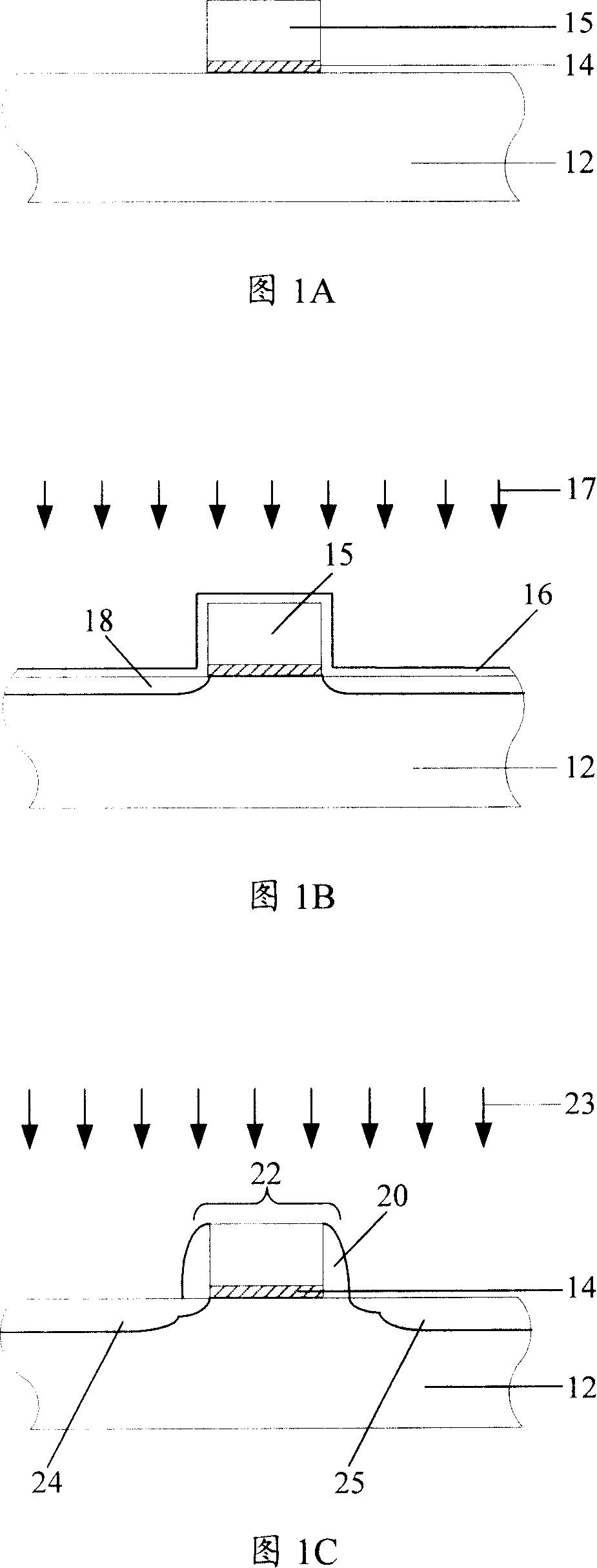
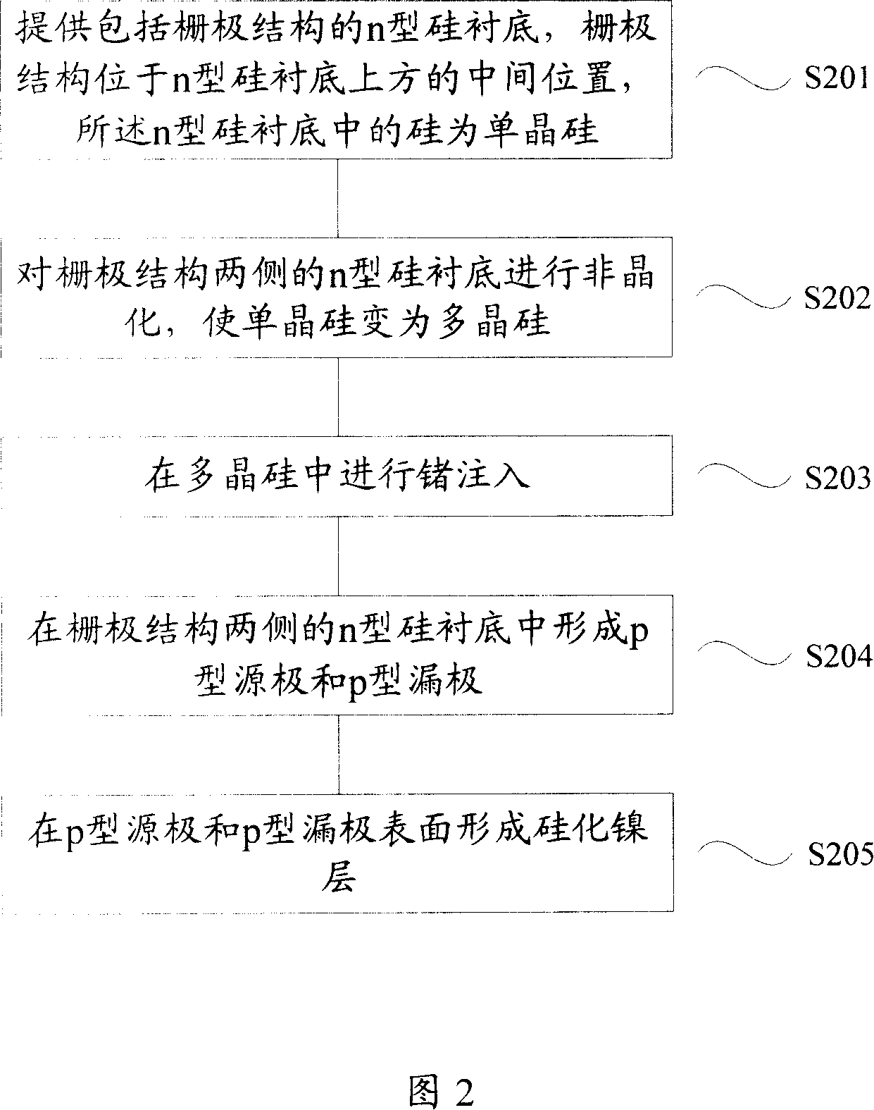
[0028] With the development of VLSI, CMOS transistors that consume less power and are suitable for high integration have been widely used in semiconductor processes. Nickel silicide is a material used in the manufacture of CMOS devices. In addition to the advantages of low resistivity and reduced silicon consumption of single silicides, it has been demonstrated that ultra-shallow junctions with plasma doping have very low junction leakage. The main obstacle to the application of nickel silicide is that nickel disilicide will be produced at the same time as nickel silicide is formed, which will form a spike and cause leakage current. Therefore, in the process of forming the PMOS transistor, especially when forming the nickel silicide layer, the present invention adds an amorphous metal implantation step so that the subsequent nickel layer reacts with the silicon substrate to form a nickel silicide layer without generating nickel disilicide , there will be no peak phenomenon, an...


PUM

PropertyMeasurementUnit
depthaaaaaaaaaa
thicknessaaaaaaaaaa
thicknessaaaaaaaaaa

Abstract

This invention relates to a method for forming SiNi2 layers and PMOS transistors, which first of all provides an n-type substrate of a grid structure to inject amorphous germanium onto the substrate , forms a source and a drain in the substrate of the two sides of the grid structure and anneals them, deposits a cover layer on the substrate and the grid structure and forms a Ni layer on the cover layer to be annealed, and the Ni layer is reacted with Si on the surface of the source and the drain to form a SiNi2 layer, eliminates unreacted Ni and cover layers to form a PMOS transistor after succeeded internal linking, in which, amorphous germanium is injected into n-type substrate before forming the source and the drain to turn monocrystal silicon in it to polysilicon then to be doped with germanium, therefore, Si2Ni4 will not be generated at the same time when the succeeded Ni layer reacts with the silicon substrate to form a SiNi2 layer nor peak phenomenon in the Si substrate.

Description

technical field [0001] The invention relates to a semiconductor device and a manufacturing method of the semiconductor device, in particular to a method for forming a P-type metal oxide semiconductor (hereinafter referred to as PMOS) transistor, and a method for improving a nickel silicide layer in the process of manufacturing the PMOS transistor. Background technique [0002] As the integration of semiconductor devices continues to increase, the critical dimensions associated with semiconductor devices continue to decrease, and low-resistivity interconnection paths become the key to fabricating dense, high-performance devices. Therefore, silicide and self-aligned silicide materials and processes have been widely used to reduce the surface resistance and contact resistance of the gate, source and drain of complementary metal oxide semiconductor (hereinafter referred to as CMOS) transistors, thereby reducing Resistor-capacitor delay time. In the known salicide technology, co...

Claims


Application Information

Patent Timeline
Patent Type & Authority Applications(China)
IPC IPC(8): H01L21/336H01L21/28
Inventor 李泽逵宁先捷
Owner SEMICON MFG INT (SHANGHAI) CORP
Why Eureka
Try Eureka