Scanning electron microscope electron back scattering diffraction in-situ stretching device and measuring method

A technology of electron backscattering and in-situ stretching, applied in measurement devices, material analysis using measurement secondary emissions, instruments, etc., can solve problems such as insufficiency, and achieve easy operation, reliable performance parameters, and easy interpretation and discovery. Effect

Inactive Publication Date: 2008-04-09
BEIJING UNIV OF TECH
View PDF0 Cites 26 Cited by
  • Summary
  • Abstract
  • Description
  • Claims
  • Application Information

AI Technical Summary

Problems solved by technology

These measurements can no longer meet the needs of current material development, especially some structural materials with micro-nano structures, such as nanocrystalline materials, thin film materials, etc.

Method used


Image

  • Scanning electron microscope electron back scattering diffraction in-situ stretching device and measuring method
  • Scanning electron microscope electron back scattering diffraction in-situ stretching device and measuring method
  • Scanning electron microscope electron back scattering diffraction in-situ stretching device and measuring method

Examples


example 1

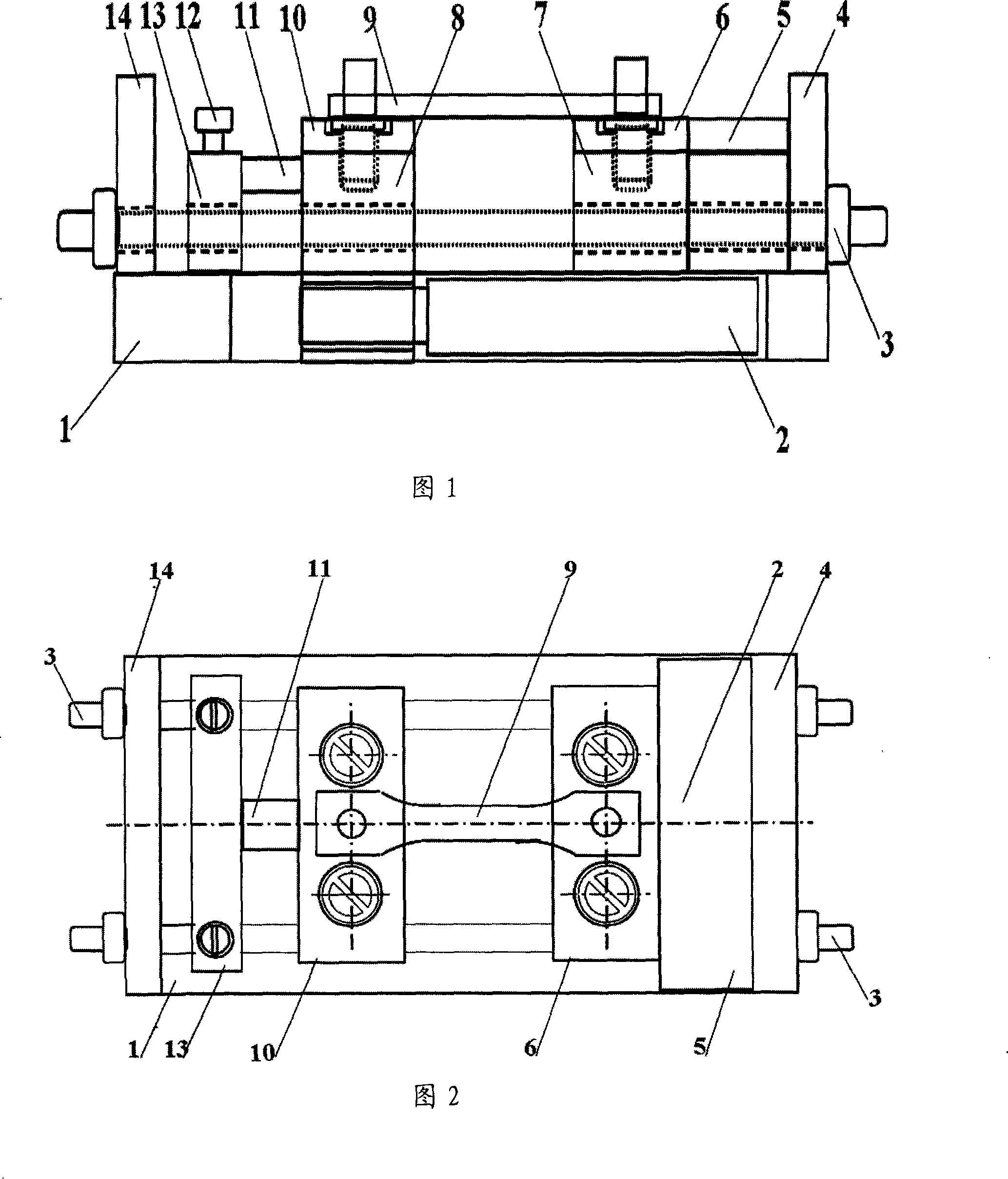
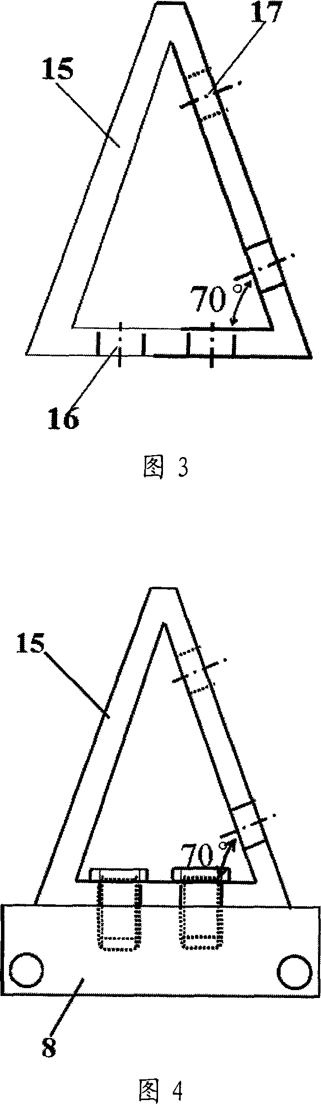
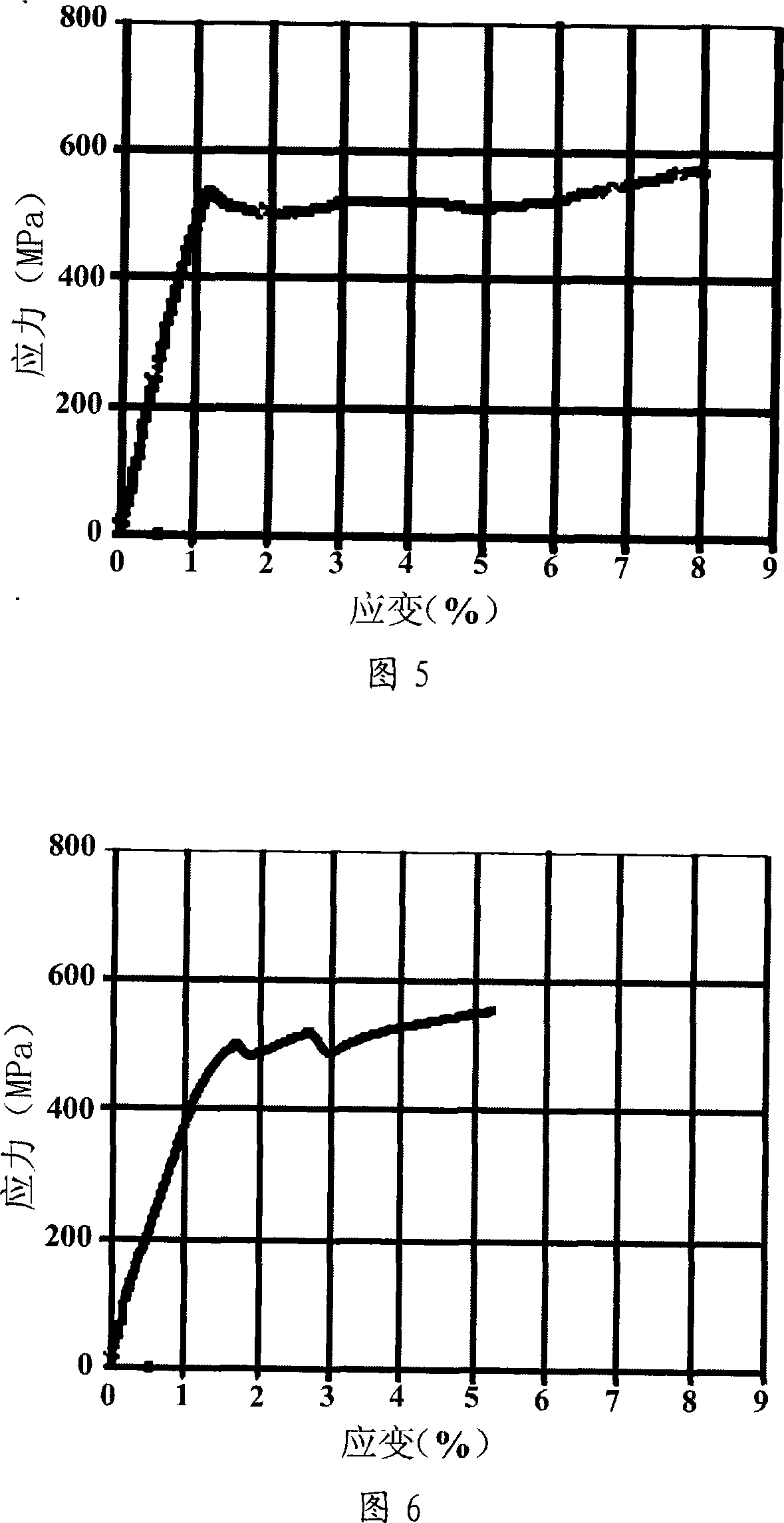
[0032]The scanning electron microscope electron backscattering diffraction in-situ stretching device is designed according to the FEI Quanta 200 environmental scanning electron microscope and the JEOL JSM 6500F field emission scanning electron microscope. The length, width and height of the device are 150mm×120mm×30mm, and the system uses a linear motor Drive, maximum loading load 500N, load accuracy 1%, piezoresistive stress sensor, maximum measurement load 5000N, accuracy 0.1N, linear displacement sensor, maximum linear displacement range 10mm, displacement accuracy 0.1μm, the device can be easily installed In the scanning electron microscope sample chamber. In the experiment, in the JEOL JSM 6500F field emission scanning electron microscope, the microscopic deformation process and the microscopic crack propagation process of the NiTi memory alloy were tested in the in-situ scanning electron microscopic imaging mode, and the NiTi memory alloy was obtained at the same time. S...


PUM


Abstract

The invention discloses a normal position stretching device of backscatter and diffraction of scanning electron microscope electron back and a test method, belonging to the material structure and capability normal position test field. The prior art is hard to be applied to the all-in-one test of the normal position microstructure and capability. The device comprises a base, a support and a drive part, a sample holding part, and a test part for stretching displacement and load. Wherein, the support part includes a fixed baffle I (4) and a fixed baffle II (14); the base (1) is sequentially provided with a sliding baffle (13), a displacing slider (8) and a stress slider (7); a pair of slide bars are fixed onto the base (1); the drive part includes a straight-line motor displacement driver (2); the sample holding part includes a loaded clamp (10) and a fixed clamp (6); and the test part for stretching displacement and load part includes a stress sensor (5), a displacement sensor (11) and a computer data collection and process system. The device provides simple structure and reliable capability, leads material mechanical property to be corresponding to the microstructure for discovering outstanding mechanical property and deformation mechanism.

Description

technical field [0001] The invention relates to a device installed in a scanning electron microscope for in-situ dynamic mechanical property testing, microscopic deformation appearance and crystal orientation observation of various solid materials. It can directly correspond the microscopic deformation mechanism and mechanical properties of various materials, and belongs to the field of in-situ testing of material structure and performance. Background technique: [0002] The macroscopic mechanical behavior of materials is a concrete manifestation of material properties and microstructure, and its mechanical performance parameters are the basic basis for the safety and reliability design of structural materials during service. Studying the microscopic deformation mechanism of materials has important theoretical significance and engineering application value for understanding the mechanical properties of materials, optimizing structural design, and developing new materials and...

Claims


Application Information

Patent Timeline
Patent Type & Authority Applications(China)
IPC IPC(8): G01N13/10G01N3/00G01N23/22
Inventor 韩晓东张跃飞毛圣成张泽
Owner BEIJING UNIV OF TECH
Why Eureka
Try Eureka