Semiconductor device and manufacturing method thereof
A manufacturing method and semiconductor technology, applied in semiconductor/solid-state device manufacturing, semiconductor devices, electric solid-state devices, etc., can solve the problems of semiconductor wafer thickness thinning, mass production performance deterioration, etc., and achieve good conduction voltage effect
- Summary
- Abstract
- Description
- Claims
- Application Information
AI Technical Summary
Problems solved by technology
Method used
Image
Examples
Embodiment Construction
[0022] Embodiments of the present invention will be described below with reference to the drawings.
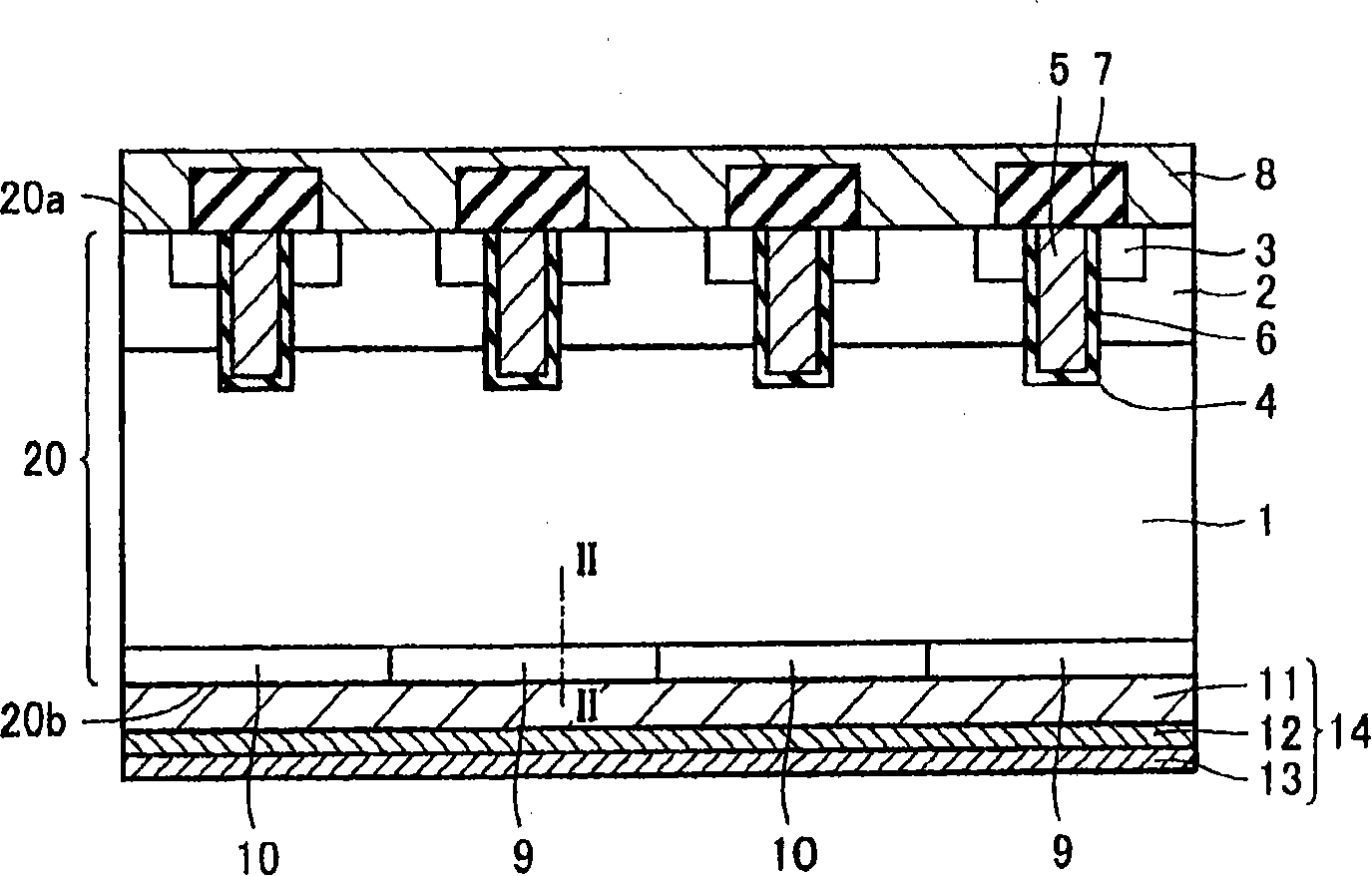
[0023] see figure 1 , the semiconductor device of the embodiment of the present invention has an IGBT and a freewheeling diode formed on a cell region of a semiconductor substrate 20 . The semiconductor substrate 20 is composed of, for example, silicon doped with n-type impurities, and has a first main surface 20 a and a second main surface 20 b facing each other. The thickness of the semiconductor substrate 20 is preferably less than 150 μm.
[0024] The IGBT mainly has a semiconductor substrate 20 n - Semiconductor layer 1, p-type base region 2, n + Emitter region 3 , trench gate 5 and p-type collector region 9 . On the unit area of the semiconductor substrate 20, in n - On the first main surface 20a side of the p-type semiconductor layer, a p-type base region 2 is selectively formed by diffusing p-type impurities. On the first main surface 20a in the p-type base reg...
PUM
 Abstract
Description
Claims
Application Information


