Silicon chip etching method

A silicon wafer and oxygen technology, applied in the manufacture of electrical components, semiconductor/solid-state devices, circuits, etc., can solve problems such as etching, affecting device performance, and deterioration of etching uniformity, and achieve sufficient etching and precise control Effect

Inactive Publication Date: 2008-05-14
BEIJING NAURA MICROELECTRONICS EQUIP CO LTD
View PDF0 Cites 0 Cited by
  • Summary
  • Abstract
  • Description
  • Claims
  • Application Information

AI Technical Summary

Problems solved by technology

When using the OES (spectral analyzer) endpoint control mode, when the SiO2 oxide layer is engraved, the spectrum of the reactant will change. At this time, the supply of the reaction gas can be stopped to effectively protect the SiO2 oxide layer. When the spectrum changes, the SiO2 oxide layer is often etched, and in the process below 0.18um, the thickness of the SiO2 layer is very thin, usually less than 50A, and the layer is easily etched away
When using the time control mode, it is di

Method used


Image

  • Silicon chip etching method
  • Silicon chip etching method

Examples


Embodiment Construction

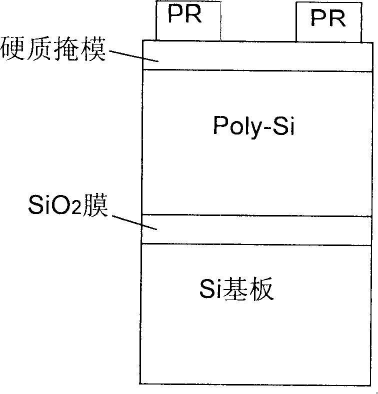
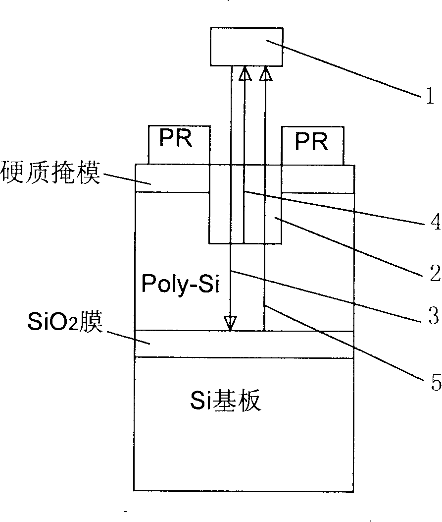
[0027] The invention is mainly used for etching the silicon chip, the silicon chip is etched by process gas, and the lower layer of the silicon chip is an oxide layer. Here poly-si (polysilicon) is taken as an example to illustrate the process of etching silicon wafers in the present invention. Below the polysilicon are SiO2 film (oxide layer), Si silicon base layer, and the top of the polysilicon is a hard mask. Above the mask is a photoresist pattern. However, the present invention is not limited to etching polysilicon, and is also used to etch other silicon wafers, and the SiO2 film in the lower layer may also be other oxide layers.

[0028] Its preferred specific implementation is, as figure 2 As shown, during the etching process of polysilicon, the IEP (laser detector) control mode is used to monitor the etching process. Specifically, the laser detector 1 is used to detect the etching process. When the etching depth is close to the upper surface of the oxide layer , to...


PUM


Abstract

The invention discloses a method for etching a silicon wafer. In the method, the silicon wafer is etched by process gas, which lower layer is an oxide layer, and the process of etching the silicon wafer is detected by a laser detector. The laser detector transmits a laser beam to an etching slot on the silicon wafer and then the lower surface of the silicon wafer and the bottom of the etching slot respectively reflect one laser beam, and thus the depth of the etching slot is analyzed by the two reflected laser beams. When the etching depth closes to the upper surface of the oxide layer or when any part of the bottom of the slot formed by etching exposes the upper surface of the oxide layer, the content of oxygen in the process gas is increased with the flow rate of oxygen of 2-50sccm in order to protect the oxide layer. Later, the process of etching can be detected by a spectrum analyzer and also estimated according to the time by experience. The invention can not only fully etch the silicon wafer but also fully protect the oxide layer beneath the silicon wafer. And the invention is especially suitable for the etching of polysilicon besides the etching of other silicon wafers.

Description

technical field [0001] The invention relates to a semiconductor silicon chip processing technology, in particular to a silicon chip etching process. Background technique [0002] At present, microelectronic technology has entered the era of VLSI and system integration, and microelectronic technology has become the symbol and foundation of the entire information age. [0003] In microelectronics technology, to manufacture an integrated circuit, it needs to go through several processes such as integrated circuit design, mask manufacturing, raw material manufacturing, chip processing, packaging, and testing. In this process, etching the semiconductor silicon wafer to form process trenches is the key technology. [0004] Reactive plasma etching refers to the method of etching under the dual effects of physical bombardment and chemical reaction of active ions on the substrate. At present, the reactive plasma etching technology has become the most widely used mainstream etching ...

Claims


Application Information

Patent Timeline
IPC IPC(8): H01L21/3065H01L21/66
Inventor 孙静
Owner BEIJING NAURA MICROELECTRONICS EQUIP CO LTD
Why Eureka
Try Eureka