Making method for organic thin film transistor
An organic thin film and manufacturing method technology, applied in semiconductor/solid-state device manufacturing, electric solid-state devices, semiconductor devices, etc., can solve problems such as poor stability, difficult transistors, and difficulty in improving device performance, and achieve the effect of improving device performance.
- Summary
- Abstract
- Description
- Claims
- Application Information
AI Technical Summary
Problems solved by technology
Method used
Image
Examples
Embodiment 1
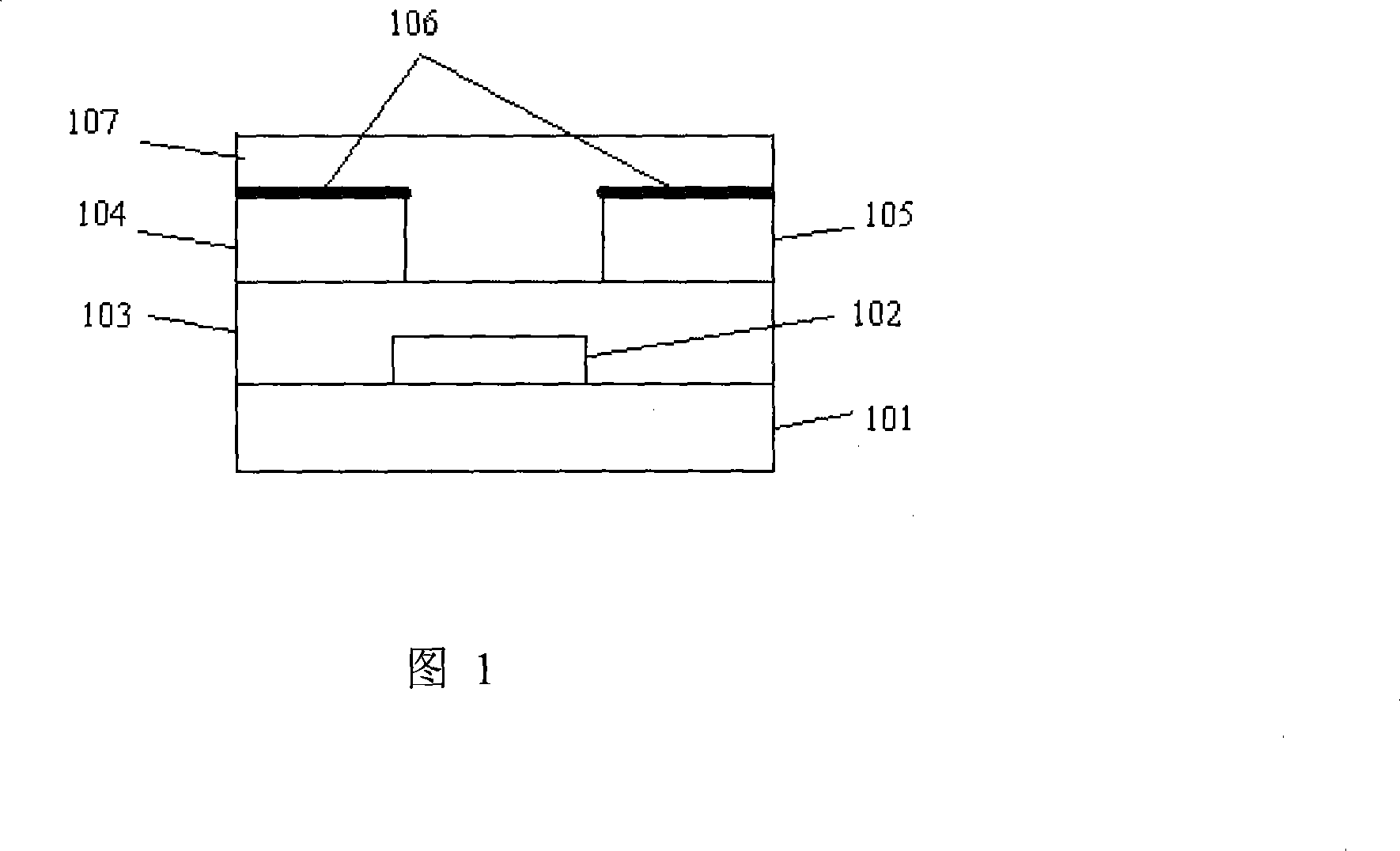
[0028] Step 1, cleaning the ITO glass sheet corroded with hydrochloric acid, the glass sheet is used as the substrate 101, and the ITO is used as the grid 102;
[0029] Step 2, plating silicon dioxide with a thickness of 250 nanometers on the ITO as the gate insulating layer 103;
[0030] The SD400M-MULTISOURCE ORGANICMOLECULAR VAPOR DEPOSITION SYSTEM inorganic coating equipment and NG-3 electron beam evaporation power supply produced by Shenyang Star Vacuum Technology Application Research Institute were used to prepare silicon dioxide films; coating conditions: system vacuum degree 9.8E-4Pa, The front stage vacuum degree is 1.0EOPa, the growth rate is 1 Ȧ / S, and the deposition time is 45 minutes;
[0031] Step 3, making the source electrode 104 and the drain electrode 105; the material used is gold, in the DEL multifunctional high vacuum system, the cavity vacuum degree is less than 3E-3Pa, and the source electrode 104 with a thickness of 70 nanometers is prepared by thermal ...
Embodiment 2
[0039] Other steps are the same as in Embodiment 1, the difference is that the material and the formation method of the organic semiconductor layer 107 are different; for the coating process of the organic semiconductor layer, TES thienyl pentacene is used, and the structural formula is
[0040]
[0041] Prepare a 4wt% toluene solution, spin-coat at 2000rpm for 60 seconds and deposit on the sheet, then anneal in air at 90°C for 2 minutes, the precursor of the pentacene derivative is converted into a pentacene film, and the organic semiconductor layer 107 is obtained. .
[0042] The structure of the organic thin film transistor is as follows: a substrate 101 , a gate 102 , a gate insulating layer 103 , a source 104 , a drain 105 , a surface modification layer 106 , and an organic semiconductor layer 107 .
[0043] Using the KEITHLEY 2410 source unit I-V test system to measure the I-V characteristic curve of organic thin film transistor devices, it is obtained that at differe...
PUM
 Abstract
Description
Claims
Application Information


