

Grids production method
A manufacturing method and gate technology, which are used in semiconductor/solid-state device manufacturing, electrical components, semiconductor devices, etc., to achieve the effects of improving efficiency, improving reliability, and reducing costs
- Summary
- Abstract
- Description
- Claims
- Application Information
AI Technical Summary
Problems solved by technology
Method used
Image

Examples
Embodiment Construction
[0036] In order to make the above objects, features and advantages of the present invention more comprehensible, specific implementations of the present invention will be described in detail below in conjunction with the accompanying drawings.
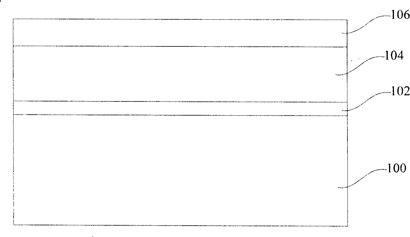
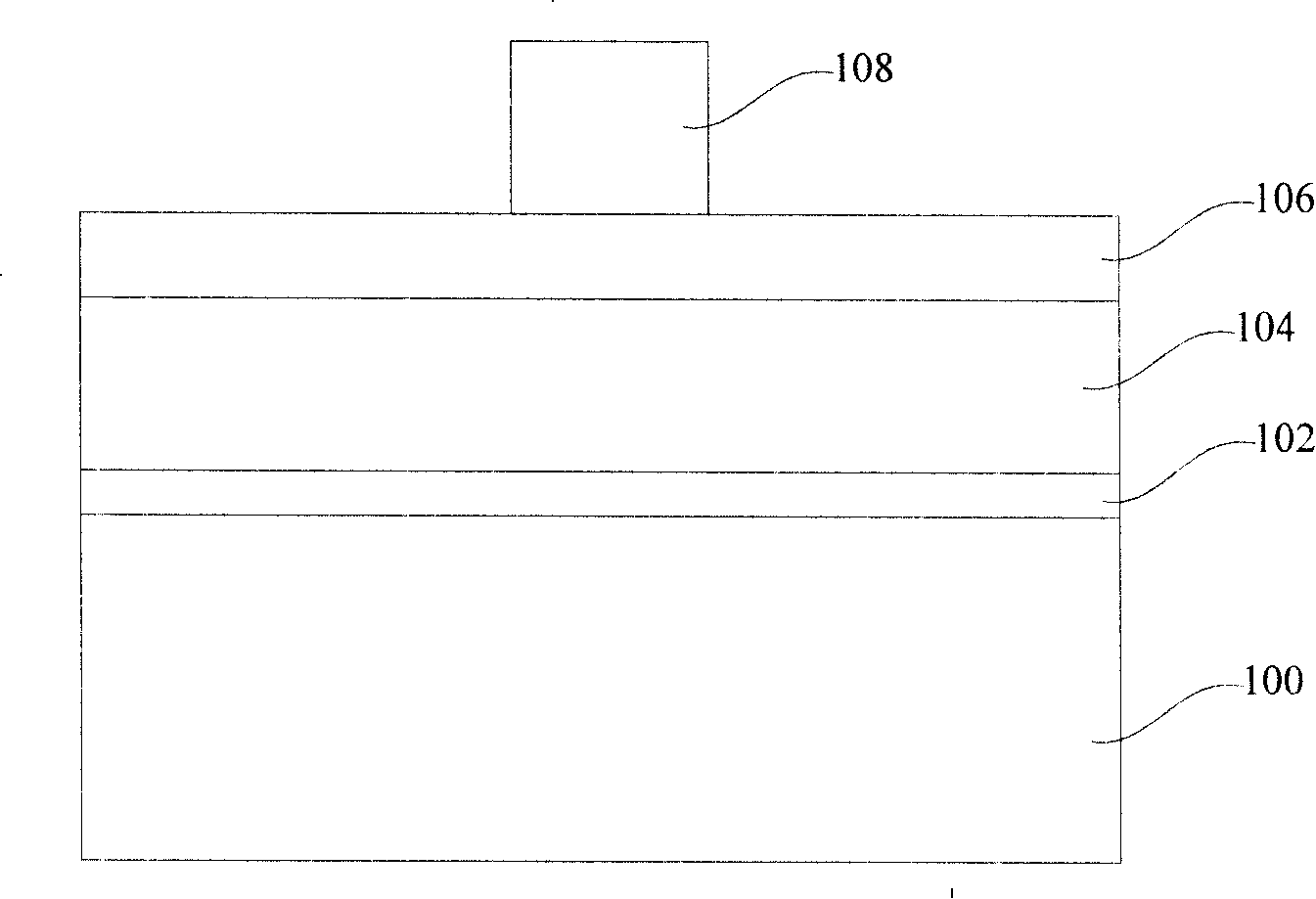
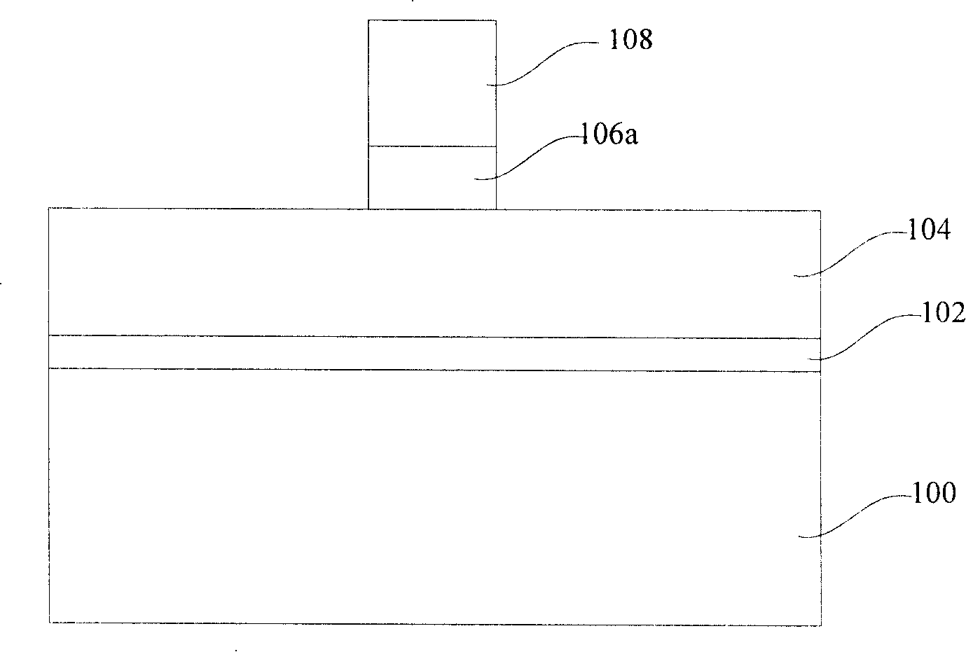
[0037] Figure 9 It is a flow chart of the first embodiment of the gate manufacturing method of the present invention. Such as Figure 9 As shown, first, a semiconductor substrate is provided, and a conductive layer is formed on the semiconductor substrate (S200). The semiconductor base material includes a semiconductor substrate and an oxide layer. The semiconductor substrate can be one of semiconductor materials such as monocrystalline silicon, polycrystalline silicon, amorphous silicon, germanium, etc., and the thickness of the oxide layer is 5 to 5. 100nm. The conductive layer is one of polysilicon, metal silicide or a combination thereof, and the method for forming the conductive layer is physical vapor deposition or chemical v...
PUM
 Abstract
Description
Claims
Application Information