Production method of metal wiring structure

A manufacturing method and metal wiring technology, which are used in semiconductor/solid-state device manufacturing, electrical components, circuits, etc., to achieve the effect of controlling contact resistance

Active Publication Date: 2008-06-11
SEMICON MFG INT (SHANGHAI) CORP +1
View PDF1 Cites 5 Cited by
  • Summary
  • Abstract
  • Description
  • Claims
  • Application Information

AI Technical Summary

Problems solved by technology

When this structure adopts the attached Figure 1A to attach Figure 1E When the metal wiring structure is formed in the above process, since the thickness of the insulating oxide layer 230 is generally greater than the etching stopper layer 240, and the surface of the isolation structure 210 is generally higher than the active region 220, when the active region 220 is completely removed After the insulating oxide layer, it will lead to over-etching of the isolation structure 210, such as Figure 2B Shown is a scanning electron microscope image of a semiconductor structure in which the isolation structure is overetched. In the accompanying drawing, both the isolation structure 210 and the active region 220 have overetching phenomena, but the overetching of the isolation structure 210 is far from much greater than the overetching of the active region 220, and the height of the overetching of the isolation structure 210 is greater than 1000 angstroms

Method used


Image

  • Production method of metal wiring structure
  • Production method of metal wiring structure
  • Production method of metal wiring structure

Examples


Embodiment Construction

[0022] The specific embodiments of the present invention will be described in detail below in conjunction with specific examples.

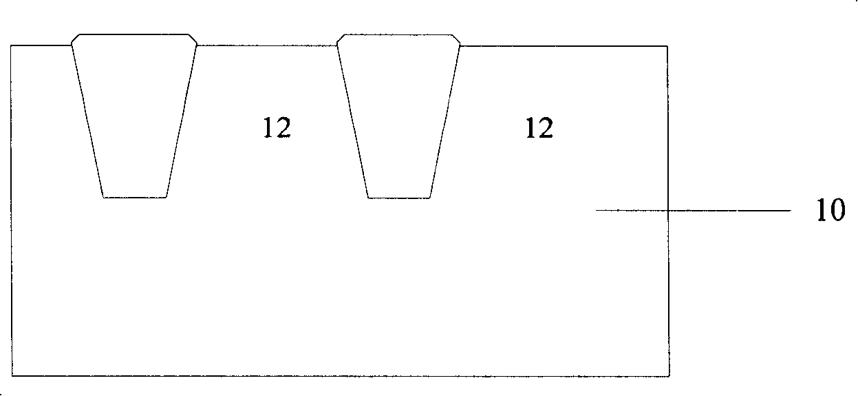
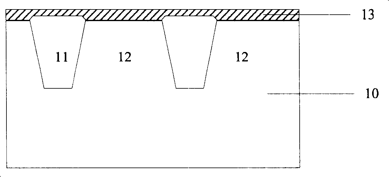
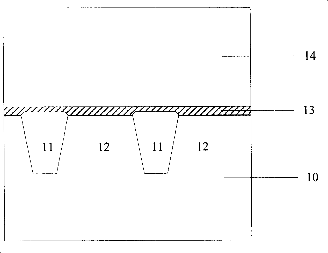
[0023] The present invention provides a method for manufacturing a metal wiring structure, which includes: providing a semiconductor substrate having an isolation structure and an active region located between the isolation structure, and the isolation structure has a corrosion barrier layer, and the active region has An insulating isolation layer; forming a first etch stop layer on the semiconductor substrate; forming a second etch stop layer on the first etch stop layer; forming an interlayer dielectric layer on the second etch stop layer; A photoresist pattern is formed on the interlayer dielectric layer; the first etching: the interlayer dielectric layer is etched with the photoresist as a mask, and stops at the second etching stop layer; the second etching: with light Resist is a mask to etch the second etch stop layer and stop at the first etch ...


PUM


Abstract

A metal wiring structure fabrication method comprises that: an active area which is provided with an isolation structure and arranged between the isolation structure; an erosion barrier layer is arranged on the isolation structure; a semiconductor substrate with an insulating layer is arranged on the active area; a first etching stop layer, a second etching stop layer and an interlevel dielectric layer are formed on the semiconductor substrate in turn; a photoresist pattern is formed on the interlevel dielectric layer; photoresist is used as mask to etch the interlevel dielectric layer and stop at the second etching stop layer; the second etching stop layer is etched till the second etching stop layer is fully removed; the photoresist is used as the mask; etching reagent which has the etching speed selection ratio between the first etching stop layer and the erosion barrier layer more than one and the etching speed selection ratio between the insulating layer and the erosion barrier layer more than one is selected; the first etching stop layer, the erosion barrier layer and the insulating layer are etched till the insulating layer and the photoresist layer on the active area are removed fully.

Description

Technical field [0001] The present invention relates to the technical field of semiconductor manufacturing, in particular to a manufacturing method of a metal wiring structure in a semiconductor device. Background technique [0002] Generally, the semiconductor manufacturing process uses deposition processes, photolithography processes, etching processes, etc. to form integrated circuit devices on silicon wafers. In order to connect various components to form an integrated circuit, a metal material with relatively high conductivity, such as copper, is usually used for wiring, that is, metal wiring. The structure used to connect the active area of ​​the semiconductor device with other integrated circuits is generally a plug structure. The process of forming a plug is a process of filling a through hole or a trench with a metal material, for example, the method of forming a plug structure provided in the Chinese patent application document with application number CN98118290. [000...

Claims


Application Information

Patent Timeline
Patent Type & Authority Applications(China)
IPC IPC(8): H01L21/768H01L21/311
Inventor 洪中山
Owner SEMICON MFG INT (SHANGHAI) CORP
Why Eureka
Try Eureka