Production method of self-aligning contact hole

A technology of self-aligned contact holes and manufacturing methods, applied in semiconductor/solid-state device manufacturing, electrical components, circuits, etc., can solve the problems of grid shoulders being cut off and the bottom of contact holes not being opened, so as to achieve good contour and engraving. The etching time is short and the effect of reducing the etching time

Active Publication Date: 2008-06-11
SEMICON MFG INT (SHANGHAI) CORP +1
View PDF1 Cites 18 Cited by
  • Summary
  • Abstract
  • Description
  • Claims
  • Application Information

AI Technical Summary

Problems solved by technology

[0013] Therefore, the purpose of the present invention is to provide a method for manufacturing a self-aligned contact hole, to solve the problems that the bottom of the contact hole is not opened and the gate shoulder is cut off in the existing method for manufacturing a self-aligned contact hole

Method used


Image

  • Production method of self-aligning contact hole
  • Production method of self-aligning contact hole
  • Production method of self-aligning contact hole

Examples


Embodiment Construction

[0036] In order to make the above objects, features and advantages of the present invention more comprehensible, specific implementations of the present invention will be described in detail below in conjunction with the accompanying drawings.

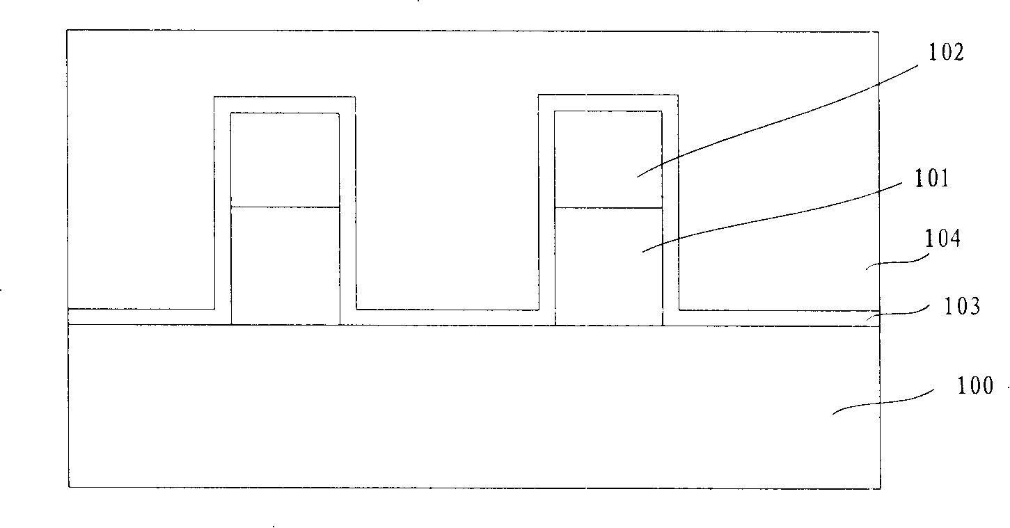
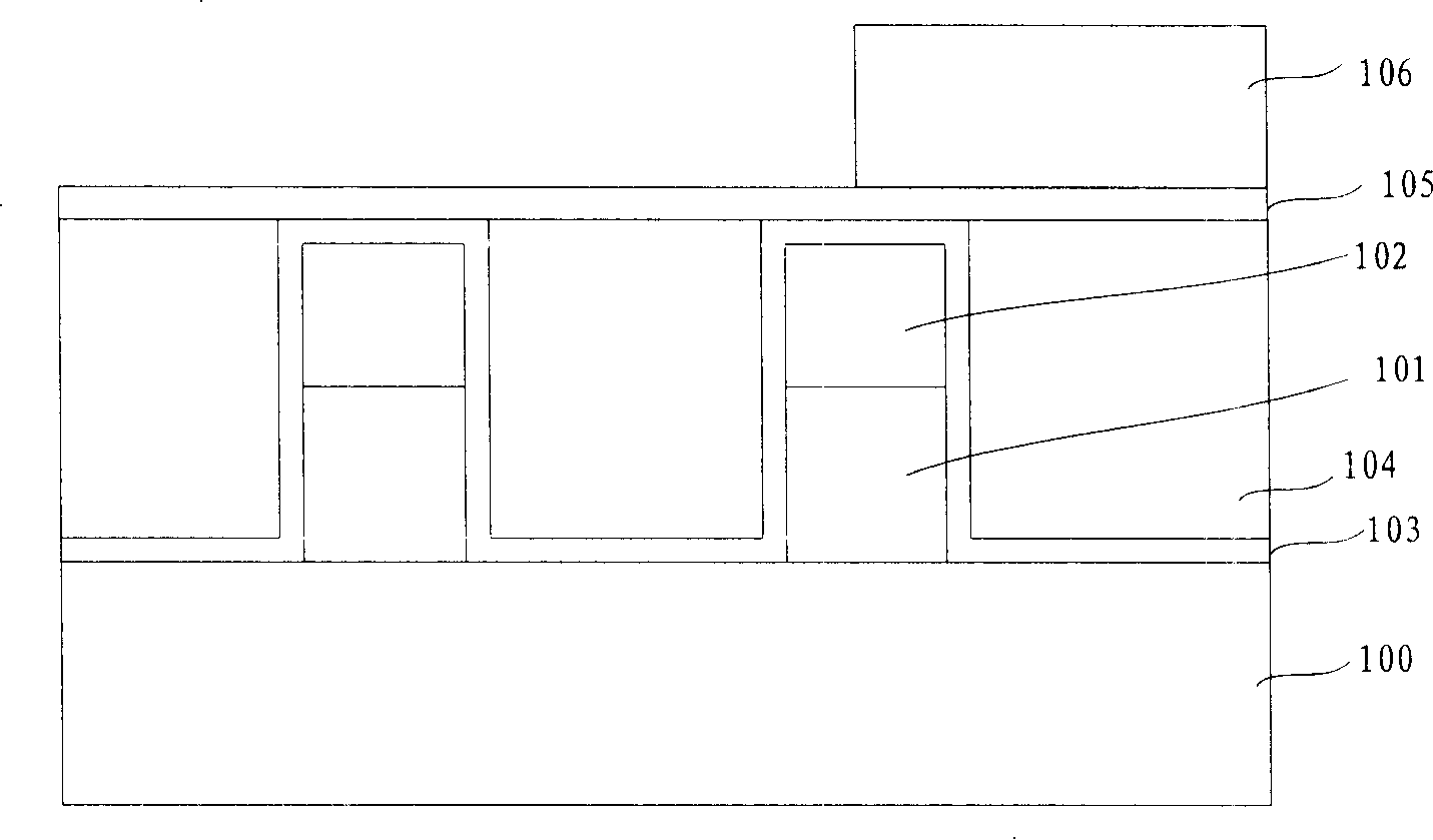
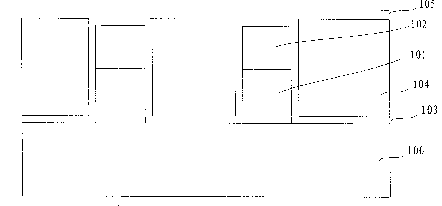
[0037] The method for manufacturing the self-aligned contact hole of the present invention firstly forms an etching barrier layer and a dielectric layer on a semiconductor substrate having at least two gate bumps, and then spin-coats a photoresist on the dielectric layer and forms a contact hole pattern , forming an opening in the dielectric layer by etching, the bottom of the opening is located between the two gates, and then cleaning the sidewall and bottom of the opening by wet method to remove the polymerization generated during etching material, and then remove the etching barrier layer on the sidewall and bottom of the opening by dry etching to form a contact hole. In the method of the present invention, the process of forming co...


PUM


Abstract

A manufacturing method of self-aligning contact holes comprises the following steps that: a semiconductor substrate is provided; at least two grid electrodes are arranged on the semiconductor substrate; an etching barrier layer is arranged along the surface of the grid electrodes; a medium layer is formed on the etching barrier layer; the top of the medium layer is higher than the top of the grid electrode; a photoresist contact hole pattern is formed on the medium layer and forms a T-shaped opening in the medium layer through etching; the bottom of the opening is arranged between two grid electrodes; the photoresist is removed; the sidewall and the bottom of the opening are cleaned through a wet method; the etching barrier layer on the sidewall and the bottom of the opening is etched and removed. The method can remove or reduce the disadvantages that in the manufacturing method of self-aligning contact holes, the bottom of the contact hole is not opened and the shoulders of the grid electrodes are cut off.

Description

technical field [0001] The invention relates to the technical field of semiconductor manufacturing, in particular to a method for manufacturing a self-aligned contact hole. Background technique [0002] With the decreasing size of semiconductor devices, more and more device units are integrated per unit area, the density of devices is gradually increasing, and the size between devices is continuously decreasing, which also increases the difficulty of manufacturing. For example, at the technology node of 90nm and below, the gap between the gates in the memory cell becomes very small, and the contact holes for connecting the source, the drain and the upper metal line are made in the gap between the gates The process becomes more difficult, and the industry introduces a method of manufacturing self-aligned contact holes to overcome this difficulty. Chinese patent application No. 200510055489.3 discloses a method of manufacturing self-aligned contact holes. Figure 1 ~ Figure 4 ...

Claims


Application Information

Patent Timeline
Patent Type & Authority Applications(China)
IPC IPC(8): H01L21/822H01L21/768H01L21/311
Inventor 吴关平陈耀祖张颂周高燕
Owner SEMICON MFG INT (SHANGHAI) CORP
Why Eureka
Try Eureka