Supercharge Your Innovation With Domain-Expert AI Agents!

CMOS image sensor and its production method

An image sensor and manufacturing method technology, applied in the field of image sensors, can solve problems such as unclear imaging, decreased photosensitivity, and reduced light energy of photodiodes, and achieve the effects of increased light energy, improved photosensitivity, and clear imaging

Active Publication Date: 2010-05-12
SEMICON MFG INT (SHANGHAI) CORP +1
View PDF4 Cites 2 Cited by
  • Summary
  • Abstract
  • Description
  • Claims
  • Application Information

AI Technical Summary

Problems solved by technology

[0010] In the prior art method for making a CMOS image sensor, due to the existence of multi-layer insulating layers and etching stop layers in the CMOS image sensor, a large amount of light is reflected and absorbed, which reduces the light energy received by the photodiode and reduces the photosensitivity. The lighting environment used by the CMOS image sensor is limited, and the image is not clear under darker environmental conditions.

Method used


Image

  • CMOS image sensor and its production method
  • CMOS image sensor and its production method
  • CMOS image sensor and its production method

Examples


Embodiment Construction

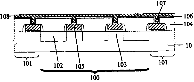
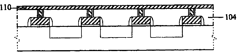
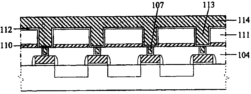
[0047] The CMOS image sensor receives light through the photodiode and converts the light signal into an electrical signal. In order to enhance the light energy received by the photodiode and improve the photosensitivity, the thin film structure of the light channel can be optimized to reduce the loss of light during propagation. . The present invention removes the multi-layer insulating layer and the etching stop layer in the image sensing area without metal connection, fills the light-transmitting resin material or directly etches the multi-layer insulating layer and the etching stop layer into a microlens, so that the light is reflected The reduced amount of absorption and absorption increases the light energy received by the photodiode and increases the photosensitivity, thereby realizing that the light environment used by the CMOS image sensor is not limited, and the imaging is clear under darker environmental conditions. In order to make the above objects, features and a...


PUM


Abstract

A CMOS image sensor comprises a silicon substrate, an insulation layer and an etching stop layer which are arranged on the silicon substrate and have dual-damascene structures, an insulation layer andan etching stop layer which are arranged on the insulation layer and the etching stop layer with dual-damascene structures and have no dual-damascene structures, a silicon dioxide layer arranged on the etching stop layer with the dual-damascene structure, a silicon oxynitride layer arranged on the silicon dioxide layer, openings which run through the silicon oxynitride layer, the silicon dioxidelayer, the etching stop layer and the insulation layer with no dual-damascene structures, an euphotic zone which is formed on the silicon oxynitride layer and is filled in the openings and a lenticuleformed on the euphotic zone of the openings. Through the procedures, a plurality of insulation layers and etching stop layers which are not communicated with metal are removed; resin material with good light transmission is filled in order to reduce the amount of the reflected and absorbed light, increase light energy received by photodiodes and improve photosensitivity, further the CMOS image sensor can achieve no limitation of lighting environment and can image clearly in a dim environmental condition.

Description

technical field [0001] The present invention relates to image sensors, and more particularly, to a CMOS image sensor with improved sensitivity and a method of manufacturing the CMOS image sensor. Background technique [0002] An image sensor receives light signals from an object and converts the light signals into electrical signals, which can then be transmitted for further processing, such as digitization, and then stored in a storage device such as a memory, optical or magnetic disk, or used in a display display, print, etc. Image sensors are commonly used in devices such as digital cameras, video cameras, scanners, facsimile machines, and the like. [0003] Image sensors are generally of two types, Charge Coupled Device (CCD) sensors and CMOS Image Sensors (CIS). CCD is called a photocoupler device, which collects charge through the photoelectric effect, and the charge of each row of pixels is sent to the analog shift register with the clock signal, and then serially c...

Claims


Application Information

Patent Timeline
Patent Type & Authority Patents(China)
IPC IPC(8): H01L21/822H01L27/146
Inventor 卢普生杨建平
Owner SEMICON MFG INT (SHANGHAI) CORP
Features
  • R&D
  • Intellectual Property
  • Life Sciences
  • Materials
  • Tech Scout
  • Unparalleled Data Quality
  • Higher Quality Content
  • 60% Fewer Hallucinations
Learn More