Method for preparation of nanometer clearance electrode

A nano-gap electrode and gap technology, which is applied in the direction of semiconductor devices, can solve problems such as difficult to realize, and achieve the effects of convenient operation, improved production efficiency, effective and precise control

Inactive Publication Date: 2008-07-23
INST OF CHEM CHINESE ACAD OF SCI
View PDF0 Cites 10 Cited by
  • Summary
  • Abstract
  • Description
  • Claims
  • Application Information

AI Technical Summary

Problems solved by technology

However, these methods still do not fully solve the problem
At present, in-situ real-time observation cannot be realized i

Method used


Image

  • Method for preparation of nanometer clearance electrode
  • Method for preparation of nanometer clearance electrode
  • Method for preparation of nanometer clearance electrode

Examples


preparation example Construction

[0025] The preparation method of the present invention is based on the principle that in a scanning electron microscope, a pre-prepared electrode is irradiated with a high-density electron beam, and the electron beam and the secondary electrons generated by it will cause complex chemical reactions to occur on the molecules adsorbed on the surface of the electrode. reaction, decomposed and deposited on the surface of the electrode, so that the electrode becomes wider and the distance between the electrodes gradually becomes smaller.

[0026] Specifically, the preparation method of the nano-gap electrode provided by the present invention utilizes electron beam induced deposition technology, and its steps are as follows:

[0027] a) Prepared by current common electrode preparation methods (such as: photolithography technology, electron beam exposure technology, current ablation technology, junction breaking technology, electrochemical deposition technology, nanowire template techn...

Embodiment 1

[0037] Taking the preparation of carbon nanotube electrodes as an example

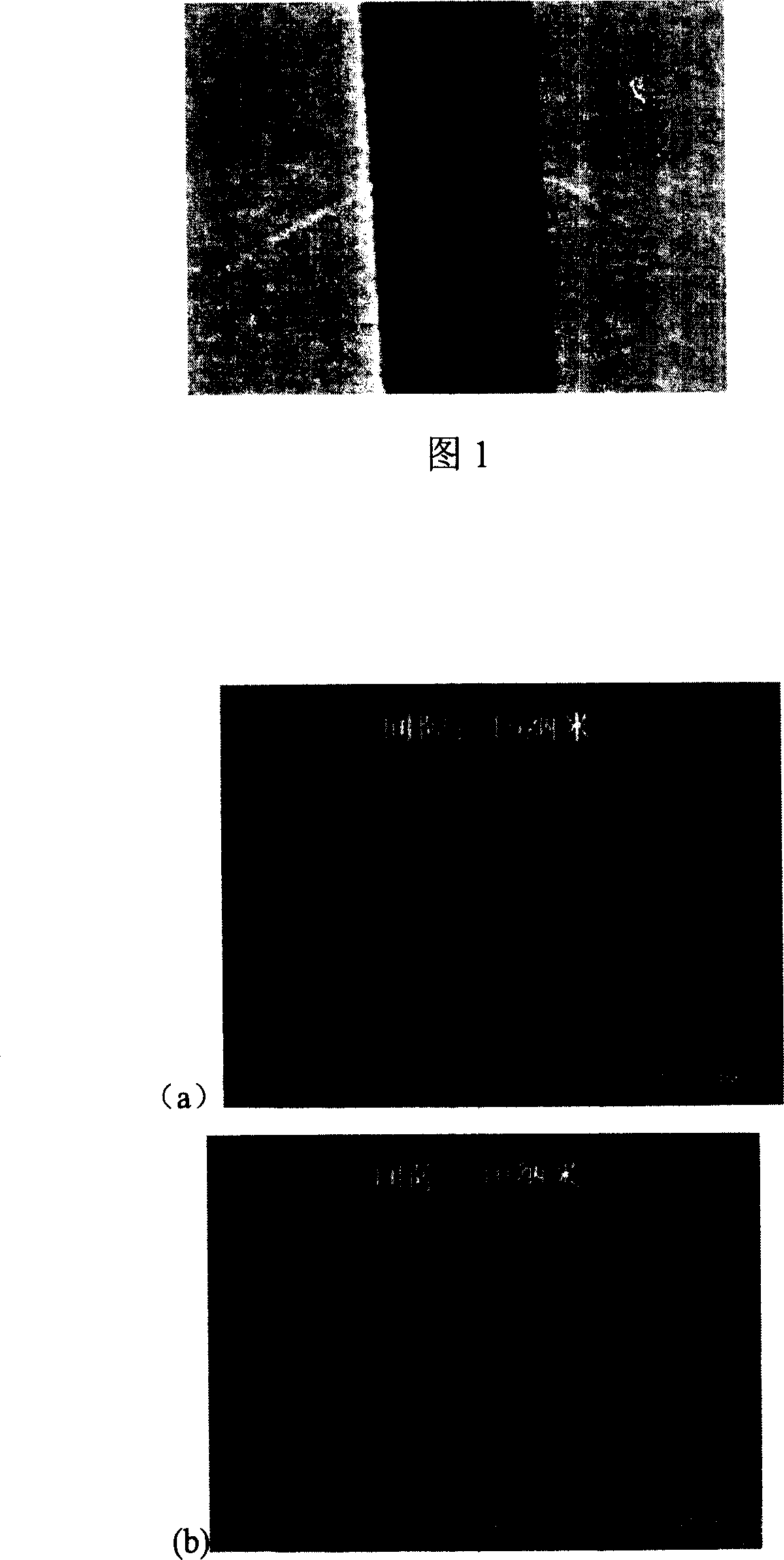
[0038] In the first step, carbon nanotubes are dispersed in an ethanol solution. Then the solution was dropped on the titanium-gold electrodes with a spacing of 2 microns, and the distribution of carbon nanotubes on the titanium-gold electrodes was observed through a scanning electron microscope. (figure 1)

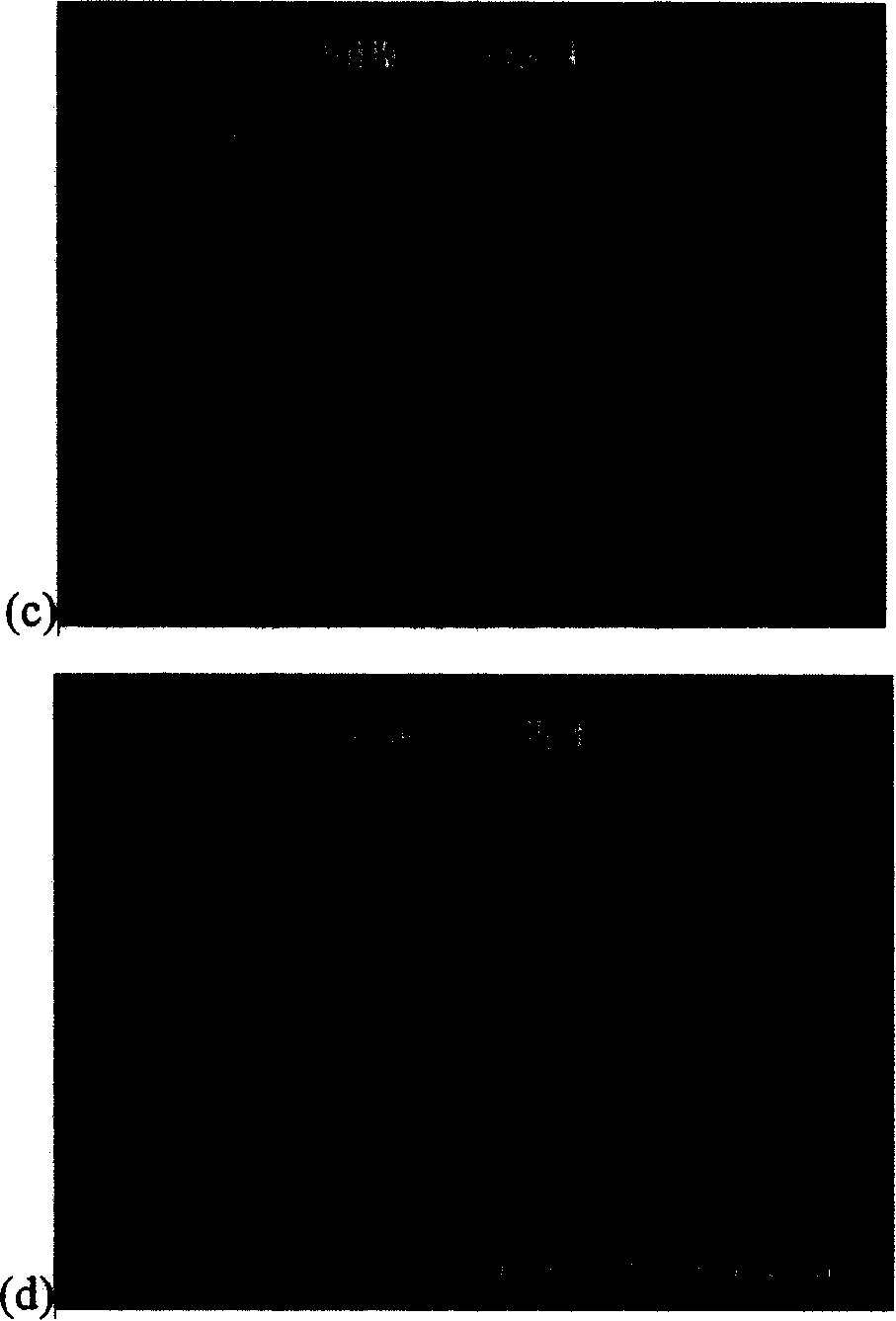
[0039] In the second step, a large voltage is applied to both ends of the titanium gold electrode connected with carbon nanotubes to burn the carbon nanotubes, thereby forming a nanoscale gap in the middle ( figure 2 a).

[0040] In the third step, the carbon nanotube electrode is placed in the vapor of toluene molecules for 1 day, so that the toluene molecules are adsorbed on the surface of the carbon nanotube electrode.

[0041] In the fourth step, the carbon nanotube electrode is placed in the scanning electron microscope, and the electron beam (energy is 15 keV, density is 10 7 Amps per sq...

Embodiment 2

[0044] According to the preparation method in Example 1, the difference is: in the third step, the carbon nanotube electrode is placed in the vapor of ethanol for 2 days. In the fourth step, the electron beam density is 2×10 6 Amperes per square meter. In the fifth step, when the electrode gap reaches 5 nanometers, stop the electron beam irradiation immediately. A carbon nanotube electrode with an electrode gap of 5 nm was prepared. Such as Figure 4 .


PUM


Abstract

A process for preparing nanometer-spaced electrodes comprises steps of preparing electrode pairs with larger gaps on nano materials which can not be destructed by electron beams, adsorbing raw material molecules induced and deposited by the electron beams on the surface of the electrode pairs, focusing the electron beams on gap areas of the electrode pairs and stopping irradiation by the electron beams to prepare and obtain the nanometer-spaced electrodes, when the gaps of the electrodes achieve the required width. Compared with the traditional process, the gaps of the electrodes can be observed in-situ in the process of preparation of the invention, thereby accurately controlling the gaps of the nanometer-spaced electrodes. Simultaneously, the invention has the advantages of convenient operation, simplicity and feasibility and high success rate, which is favorable for increasing preparing efficiency of the nanometer-spaced electrodes. The prepared nanometer-spaced electrodes have quite wide gap range from 2 nanometers to 100 nanometers, which is extremely significant for the control and application of nano and molecular devices.

Description

technical field [0001] The invention relates to a preparation method of a nano-electrode, in particular to an electron beam-induced deposition method for preparing a nano-gap electrode. Background technique [0002] Molecular electronic devices, as the next generation of electronic devices, have always been a research hotspot in the scientific community in the past ten years. A series of significant progress has been made in recent years, but some problems have not been effectively resolved, hindering the further development of molecular electronics. Among them, the preparation of nano-gap electrodes is an urgent problem to be solved. Because the first step in the realization of molecular electronics is to prepare molecular gap electrodes, so that the gap between the electrodes is just consistent with the size of the molecules to be connected. Many researchers are studying how to solve this difficult problem. At present, there have been some relatively successful methods t...

Claims


Application Information

Patent Timeline
IPC IPC(8): H01L21/28
Inventor 刘云圻魏大程曹灵超李祥龙王钰张洪亮石大川于贵
Owner INST OF CHEM CHINESE ACAD OF SCI
Why Eureka
Try Eureka