Processing method of GaN basis light emitting diode surface coarsing

A technology for light-emitting diodes and surface roughening, which is applied to electrical components, circuits, semiconductor devices, etc., can solve the problems of inconspicuous surface roughening, increased processing complexity, irregular surface undulations, etc., to increase the number of corrosion pits, The effect of good roughening effect, enhancing effect

Inactive Publication Date: 2008-07-23
XIDIAN UNIV
View PDF0 Cites 23 Cited by
  • Summary
  • Abstract
  • Description
  • Claims
  • Application Information

AI Technical Summary

Problems solved by technology

Due to the high chemical stability of GaN on the Ga polar surface, a large number of experiments have shown that KOH solution cannot corrode it, so the effect of this method is not very obvious, especially for the p-type GaN layer with high crystal quality
Strong acid solution can selectively corrode GaN at the dislocation surface outcrop on the Ga polar surface, but the roughening effect will be r

Method used


Image

  • Processing method of GaN basis light emitting diode surface coarsing
  • Processing method of GaN basis light emitting diode surface coarsing
  • Processing method of GaN basis light emitting diode surface coarsing

Examples


Embodiment Construction

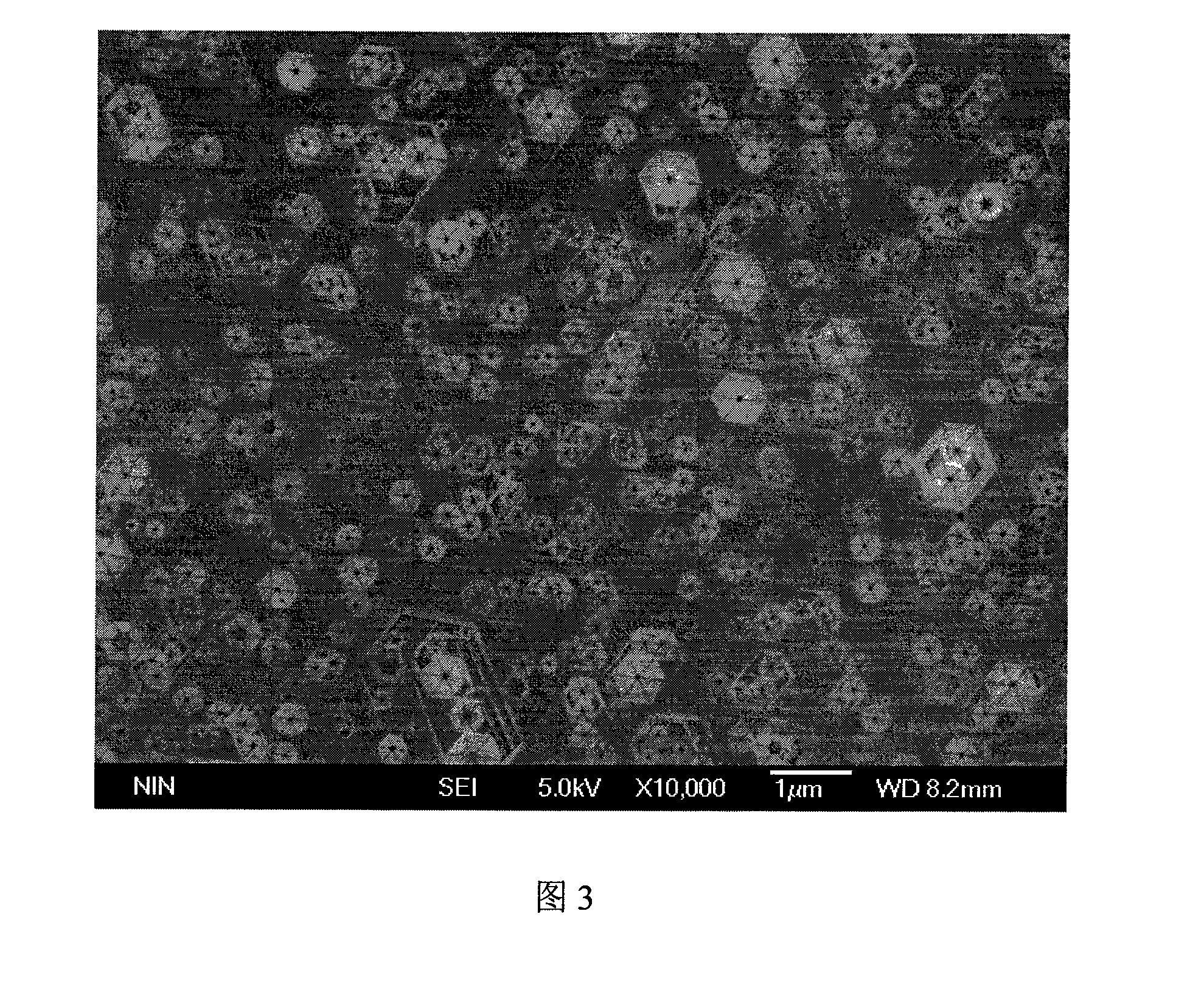
[0023] Referring to FIG. 1 , it is a schematic diagram of the GaN-based LED surface roughening treatment process of the present invention. Its specific implementation process is described as follows:

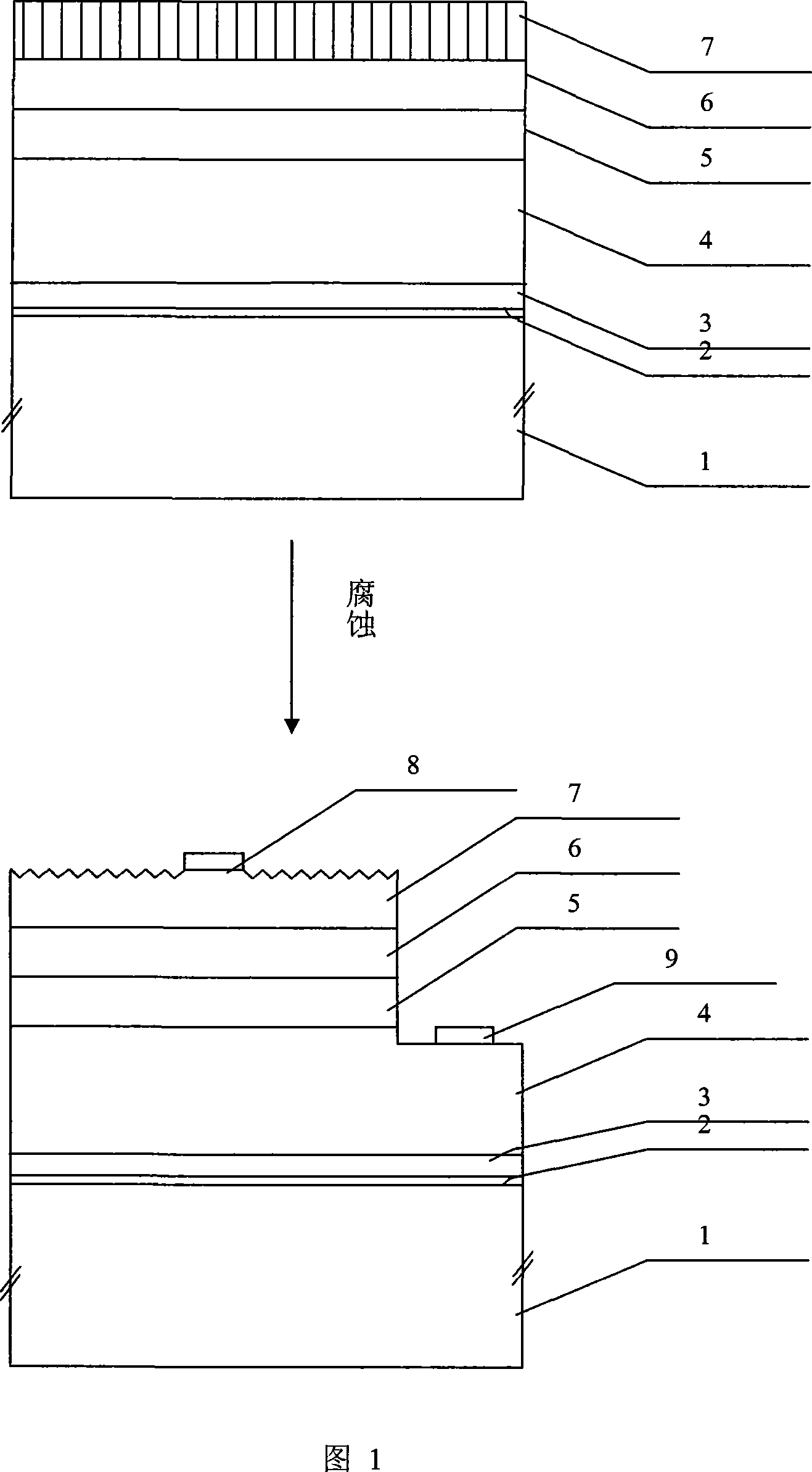
[0024] 1. Grow the p-type GaN cap layer in the GaN-based LED epitaxial wafer at a low temperature of 600°C to 750°C, so that the dislocation of the cap layer propagates in the direction perpendicular to the epitaxial surface without bending, so that the cap The dislocation density of the layer increases without affecting the optoelectronic properties of the device. The upper figure in Figure 1 is a schematic cross-sectional view of the GaN-based LED epitaxial wafer structure with low-temperature p-GaN as the cap layer. The vertical line in the cap layer in the figure indicates that this layer contains a large number of dislocations that propagate perpendicular to the surface.

[0025] 2. Under the set etching temperature and time, the LED epitaxial wafer is etched with molten K...


PUM

PropertyMeasurementUnit
Thicknessaaaaaaaaaa

Abstract

The invention discloses a processing method of coarsening the surface of a GaN based lighting diode, which relates to the technical field of preparing semiconductor optoelectronic devices. The aims are that under the state that other photoelectric characteristics of the devices are not affected, and the light removal rate is improved using the method. The implementation procedure of the method are that V1ing, a P type GaN cap layer in an extension wafer of the GaN based lighting diode grows in a low temperature of 600-750 DEG C, the dislocation of the cap layer is spread along a direction which is perpendicular to an extensional surface, the bend does not produce, thereby increasing the dislocation density of the cap layer and not affecting the photoelectric characteristics of the devices. V2ing, the extension wafer of the lighting diode is eroded by melted KOH in a given corrosion temperature and time, the high-density dislocation which is perpendicular to the extensional surface in the P type GaN layer is optionally eroded, and dense corrosion pits whose shapes are regular are formed on the surface of the device. The processing method is capable of improving the luminous efficiency of the device.

Description

technical field [0001] The invention relates to the technical field of manufacturing semiconductor optoelectronic devices, in particular to a method for roughening the surface of a GaN-based light-emitting diode (LED), which can be used to improve the luminous efficiency of the device. Background technique [0002] GaN-based light-emitting diodes (LEDs) are widely used in the fields of display technology and solid-state lighting due to their excellent characteristics such as long life, high reliability, high efficiency and energy saving. At present, the luminous efficiency of GaN blue LED is several lumens / watt, and the luminous efficiency of GaN white LED, that is, blue light + phosphor is usually tens of lumens / watt, which is comparable to incandescent lamps, but still lower than the level of fluorescent lamps. Therefore, how to improve luminous efficiency has become a major technical bottleneck faced by GaN-based LEDs. [0003] There are two ways to improve the luminous ...

Claims


Application Information

Patent Timeline
IPC IPC(8): H01L33/00H01L33/22
Inventor 李培咸高志远郝跃周小伟
Owner XIDIAN UNIV
Why Eureka
Try Eureka