Forming method for micro crystal silicon film

A hydrogenated microcrystalline silicon and thin-film technology, which is applied in photovoltaic power generation, electrical components, climate sustainability, etc., can solve problems such as difficulty in ensuring uniformity, microcrystalline silicon solar cells not having low-cost competitiveness, and consumption

Inactive Publication Date: 2008-08-06
BEIJING XINGZHE MULTIMEDIA TECH
View PDF0 Cites 12 Cited by
  • Summary
  • Abstract
  • Description
  • Claims
  • Application Information

AI Technical Summary

Problems solved by technology

[0006] Although microcrystalline silicon is a potential material for thin-film solar cells, its current obvious disadvantages are the lengthy and complicated process of its growth, and the need to use sophisticated and expensive plasma deposition equipment, the productivity is very low, and it consumes a large amount of high-purity silicon. The source gas (mainly hydrogen), especially in large-area coating, its uniform...

Method used


Image

  • Forming method for micro crystal silicon film
  • Forming method for micro crystal silicon film

Examples


Embodiment Construction

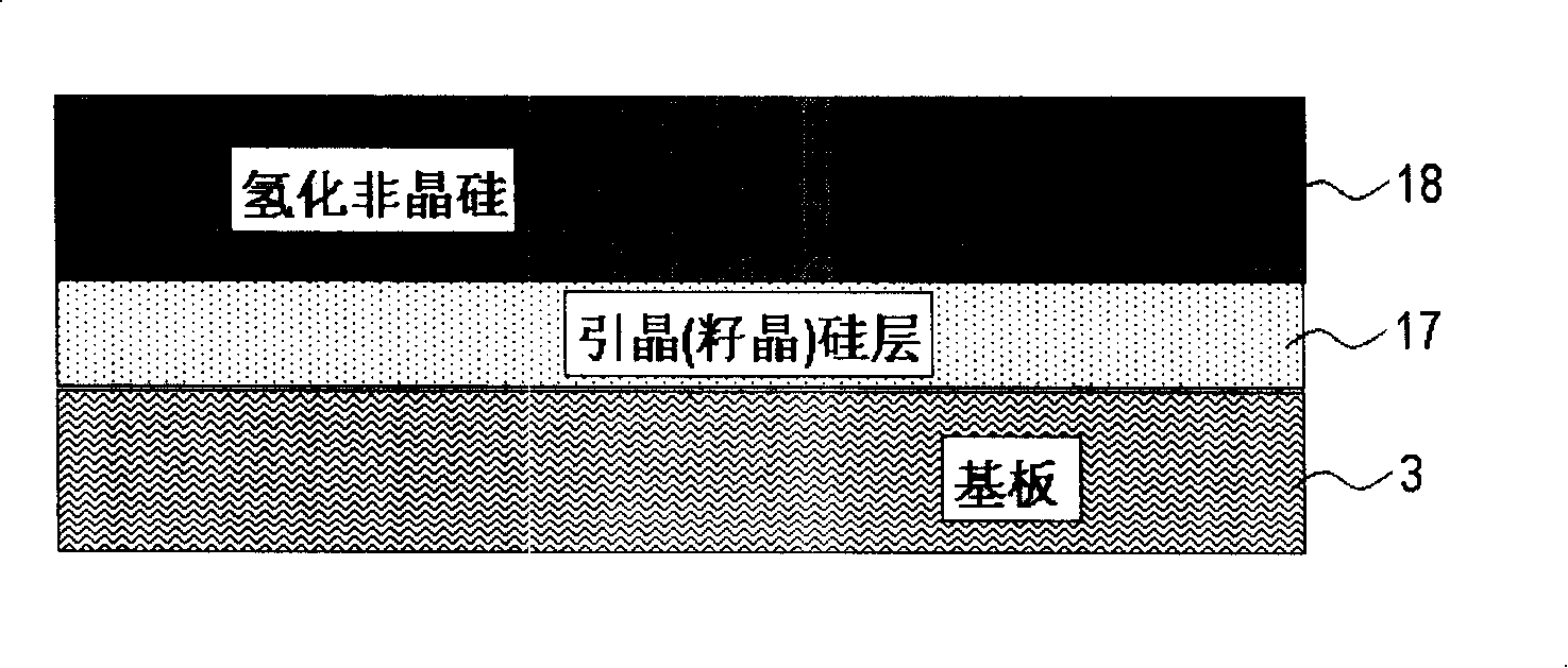
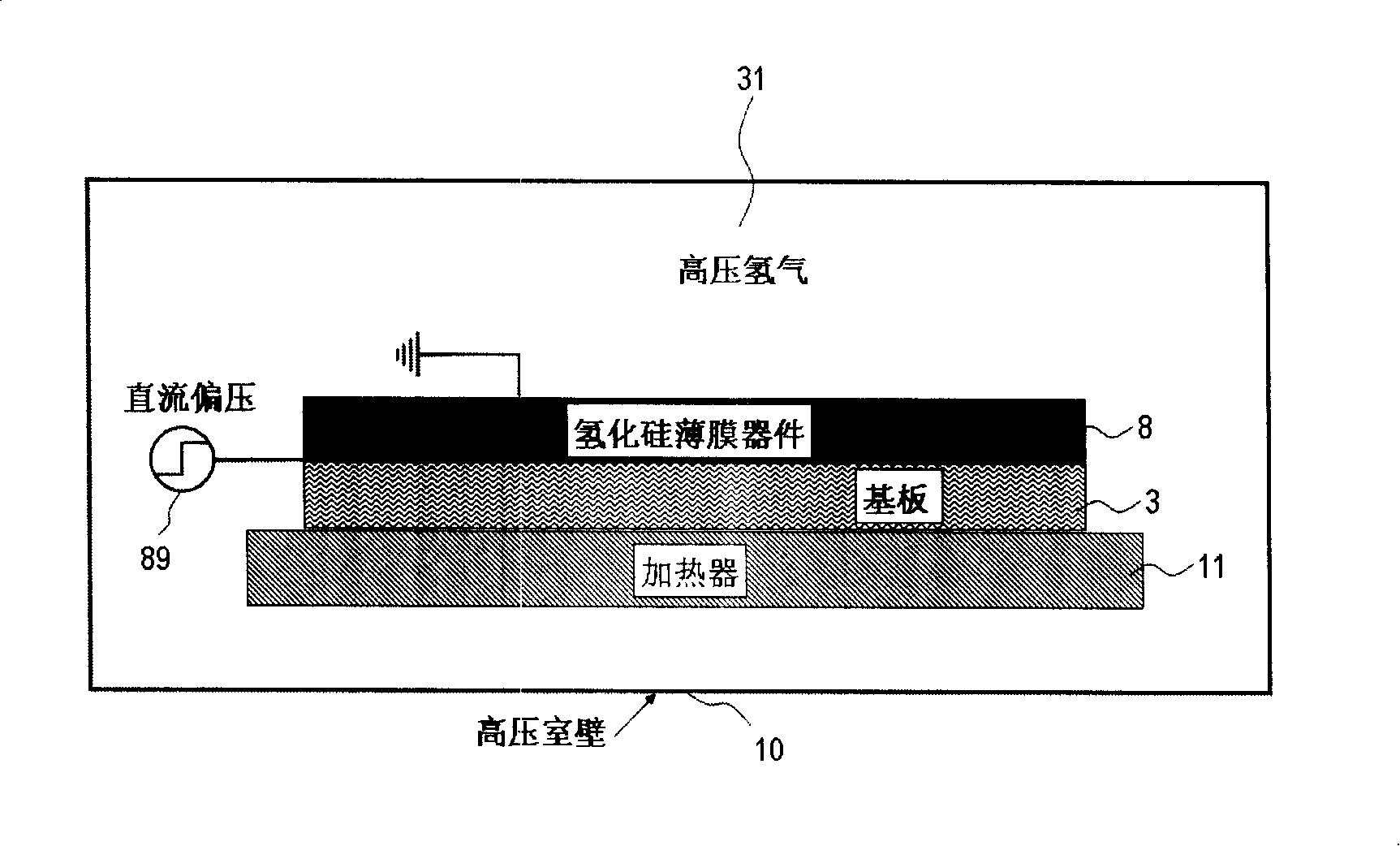
[0013] The present invention employs a two-step process to obtain high-quality microcrystalline silicon. The first step is to use the method of plasma enhanced chemical vapor deposition to obtain a hydrogenated amorphous silicon film with a seed layer at the bottom on the substrate, the growth rate of the amorphous silicon film is not lower than 1 nm / s, and the thickness is not more than 3 Microns. The second step is as figure 2 As shown, the silicon hydride material 8 placed on the substrate 3 is placed on a support base 11 with a heating function in the high-pressure chamber 10, and a high-pressure hydrogen gas 31 of not less than 500 atmospheres is introduced into the high-pressure chamber. At a temperature of 300°C, the material is annealed for 3-10 hours to obtain hydrogenated microcrystalline silicon suitable for photoelectric conversion. During the high pressure medium temperature annealing process, if the hydrogenated silicon film is placed in a device, a DC bias vo...


PUM

PropertyMeasurementUnit
Thicknessaaaaaaaaaa
The average particle sizeaaaaaaaaaa

Abstract

The present invention discloses a method for manufacturing a hydrogenated microcrystalline silicon film. Firstly a hydrogenated microcrystalline silicon seeding layer having a crystal nucleus is formed on a substrate, and then a hydrogenated amorphous silicon film with a thickness of no more than 3 micrometers is formed quickly by a plasma chemical vapor deposition method. Afterwards the material is put under high pressure hydrogen circumstance which is no less than 500 atmospheres, and at temperature no more than 300 DEG.C, the duration is 3 to 10 hours, thereby the hydrogenated microcrystalline silicon suitable for photoelectric conversation is obtained.

Description

technical field [0001] The invention belongs to the field of semiconductor material preparation, and in particular relates to the preparation technology of thin-film solar cell materials. Background technique [0002] Solar photovoltaic power generation is one of the important ways to obtain renewable energy that is beneficial to the environment. In recent years, thin-film photovoltaic cells and large-area photovoltaic modules have attracted more and more attention from the world. In particular, hydrogenated amorphous silicon, nanocrystalline silicon, and microcrystalline silicon have shown great potential with the wide application of photovoltaic devices in commercial and residential installations. A notable feature of producing thin-film silicon photovoltaic devices at a relatively low temperature below 260°C is that semiconductor films and electrical contact films with excellent performance related to silicon can be deposited on a large area. At the same time, substrates...

Claims


Application Information

Patent Timeline
IPC IPC(8): H01L31/18H01L21/20H01L31/0368H01L31/042
CPCY02E10/50Y02P70/50
Inventor 李沅民马昕
Owner BEIJING XINGZHE MULTIMEDIA TECH
Why Eureka
Try Eureka