
Thermal drive deforming transmission electric mirror grid and one-dimensional nano material deforming method

A technology of transmission electron microscopy and nanomaterials, which is applied in the direction of circuits, discharge tubes, electrical components, etc., can solve the problems of application limitations, poor controllability, and poor controllability of curling, and achieve the effects of simple structure, convenient installation, and reliable performance

Inactive Publication Date: 2008-08-27
BEIJING UNIV OF TECH
View PDF0 Cites 11 Cited by
  • Summary
  • Abstract
  • Description
  • Claims
  • Application Information

AI Technical Summary

Problems solved by technology

However, the controllability of the curling of the carbon film induced by electron beam irradiation is poor, the application of stress and the strain rate are difficult to control, and the stress provided is limited, and it is difficult to deform some materials with high strength.
[0006] In the above-mentioned in-situ nanomaterial mechanical property test by transmission electron microscope, neither the first two sample consoles nor the carrier grid can achieve large-angle double-tilt. For most nanomaterials that require real-time observation of structural changes under the action of external forces , its application is limited by
While the third method is less controllable and provides limited stress, many materials are not suitable for this method

Method used


Image

  • Thermal drive deforming transmission electric mirror grid and one-dimensional nano material deforming method
  • Thermal drive deforming transmission electric mirror grid and one-dimensional nano material deforming method
  • Thermal drive deforming transmission electric mirror grid and one-dimensional nano material deforming method

Examples


Embodiment

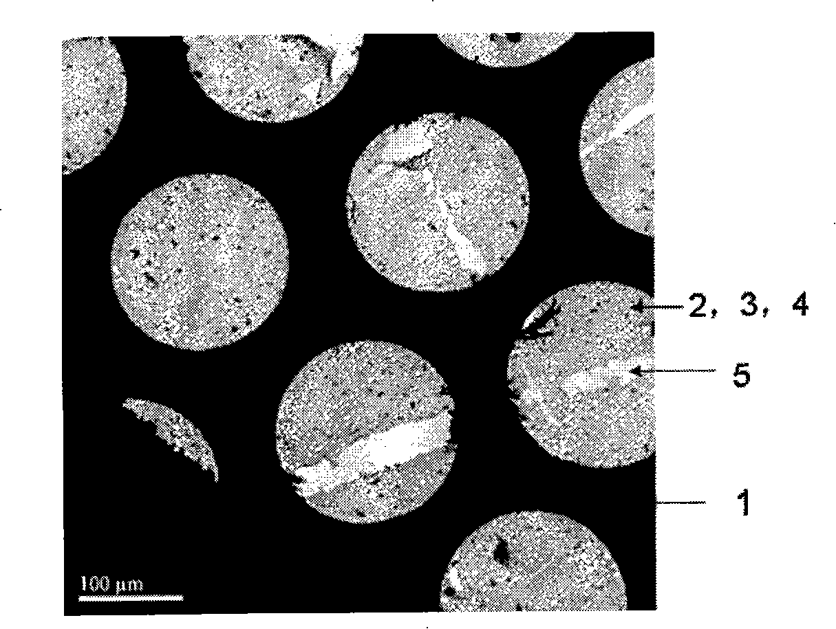
[0025] Using the conventional physical evaporation coating process to make thermally driven deformable transmission electron microscope grids, such as figure 1 As shown, a support film (2) (carbon film) is laid on the skeleton (1) (copper mesh), and a metal film A (3) and a metal film B (4) are vapor-deposited on the upper surface of the support film (2) in sequence; Wherein, the metal film A (3) is made of Mn72Ni10Cu18 alloy, the metal film B (4) is made of Ni36Fe64 alloy, the thickness of the metal film A (3) is 30nm, and the thickness of the metal film B (4) is 30nm.

[0026] Deformation of one-dimensional nanomaterials using thermally driven deformable TEM grids:

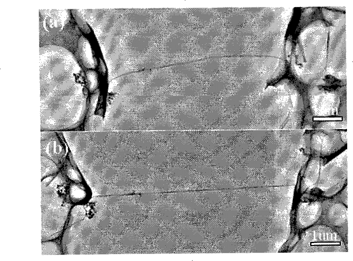
[0027] 1) Prefabricate some microcracks (5) on the metal films A (3) and B (4) of the grid with a blade, such as figure 2 As shown, the black area is the skeleton (1) (copper mesh), the gray round hole area is the support film (2) (carbon film), metal film A (3) and metal film B (4), and the blank area is the ...


PUM

PropertyMeasurementUnit
Thicknessaaaaaaaaaa

Abstract

The invention relates to a thermally driven deforming transmission electron microscope grid and a one-dimensional nano material deformation method, belonging to the nano device and the transmission electron microscope original position nano material deformation method field. The prior grid can be deformed only through electron beam irradiation and the stress supplied is limited. The grid of the invention is as follows: a metallic film A and a metallic film B are vapor-plated on a supporting film of the prior grid, and the thermal expansion coefficient of the metallic film A is more than that of the metallic film B. The one-dimensional nano material deformation method by adoption of the grid is as follows: after the metallic film A and the metallic film B are cut open, one-dimensional nano materials are dispersed on the metallic film A and the metallic film B which are then placed into a transmission electron microscope for heating; the two cracked films are curled due to difference of the expansion coefficients, thereby the driving force for deformation of the one-dimensional nano materials is provided and deformation of the one-dimensional nano materials is realized. The grid can realize large-angle roll steer in two directions of X and Y and realize the original position deformation operation of the one-dimensional nano materials; moreover, the grid is characterized in reliable performance, convenient assembly and simple structure and expands the function of the transmission electron microscope.

Description

technical field [0001] The invention belongs to the field of in-situ nano material deformation methods in nano devices and transmission electron microscopes, and in particular relates to a heat-driven deformation transmission electron microscope grid and a one-dimensional nano material deformation method. Background technique [0002] Due to the extremely high resolution of the transmission electron microscope, it can provide information at the nanoscale or even the atomic scale. It is a powerful tool for studying the microstructure of substances. It has a wide range of applications in physics, chemistry, material science, life science and other fields, especially in the current The rapidly developing field of nanoscience and technology is one of the most powerful research tools. The transmission electron microscope grid is used to support the sample to be tested. The skeleton of the most commonly used transmission electron microscope grid is generally a copper grid, and the...

Claims


Application Information

Patent Timeline
IPC IPC(8): H01J37/20G01N1/28
Inventor 韩晓东郑坤张泽
Owner BEIJING UNIV OF TECH
Learn More