Method for cleaning polycrystalline silicon gate surface

A polysilicon gate, surface deposition technology, applied in electrical components, semiconductor/solid-state device manufacturing, circuits, etc., can solve problems affecting device yield and other issues, and achieve the effect of improving yield, reducing defects, and improving adhesion performance

Active Publication Date: 2008-08-27
SHANGHAI HUAHONG GRACE SEMICON MFG CORP
View PDF0 Cites 10 Cited by
  • Summary
  • Abstract
  • Description
  • Claims
  • Application Information

AI Technical Summary

Problems solved by technology

Therefore, the P concentration in the polysilicon body and surface forms a gradient, and the doped P will continue to diffuse to the surface. As time goes by, more and more metaphosphoric acid crystals are formed on the polysilicon surface. Seriously affect the yield of the device

Method used


Image

  • Method for cleaning polycrystalline silicon gate surface
  • Method for cleaning polycrystalline silicon gate surface

Examples


Embodiment Construction

[0008] The preferred embodiments of the method for cleaning the surface of the polysilicon gate of the present invention are described below in order to further understand the purpose, specific structural features and advantages of the present invention.

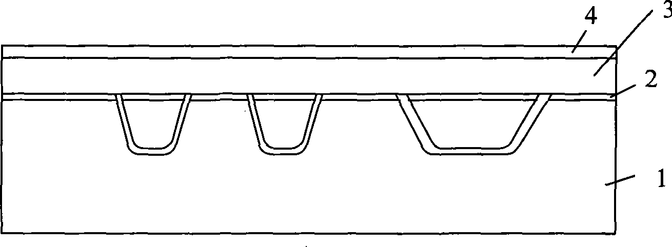
[0009] figure 1 It is a partial cross-sectional structure diagram of a silicon wafer for making a MOS device. The silicon wafer includes a substrate 1 , a gate oxide layer 2 and a polysilicon gate 3 formed on the substrate 1 . In order to improve the conductivity of the polysilicon gate 3 , it is necessary to deposit a tungsten silicide layer 4 on the surface of the polysilicon gate 3 . In order to improve the adhesion performance between the polysilicon gate 3 and the tungsten silicide layer 4 , before depositing the tungsten silicide layer 4 , it is necessary to perform the cleaning method provided by the present invention on the surface of the polysilicon gate 3 .

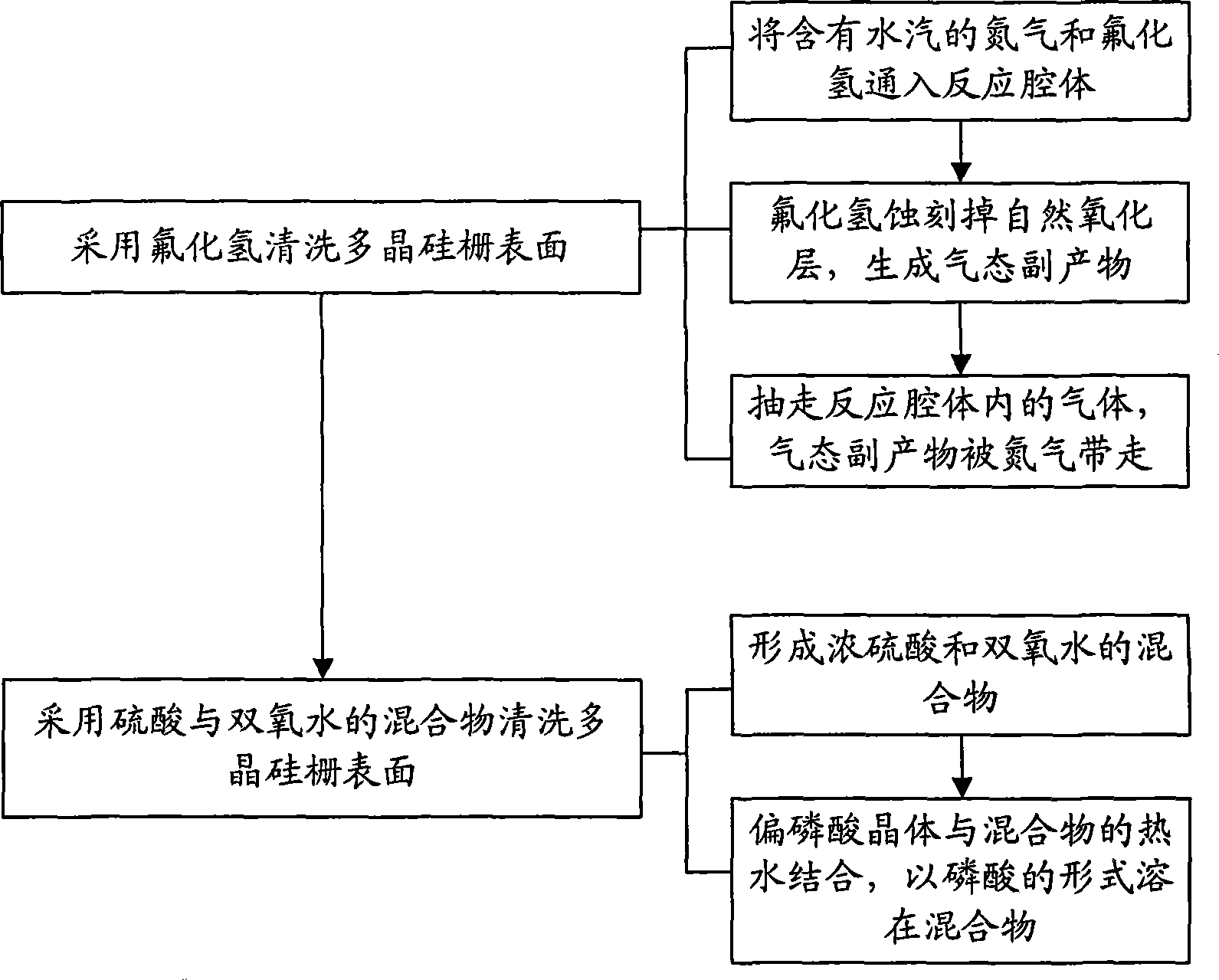
[0010] see figure 2 combine figure 1 The cleaning m...


PUM


Abstract

The invention discloses a cleaning method for a multicrystal silicon gate, which is applied before a tungsten silicide layer is deposited on the surface of the multicrystal silicon gate. The prior cleaning method can not remove metaphosphoric acid crystals on the surface of the multicrystal silicon gate, thereby the yield rate of devices is affected. The cleaning method of the invention adopts hydrogen fluoride to clean the surface of the multicrystal silicon gate and adopts mixture of sulfuric acid and hydrogen peroxide solution to clean the surface of the multicrystal silicon gate. By adoption of the cleaning method provided by the invention, autoxidation layers and the metaphosphoric acid crystals which are formed on the surface of the multicrystal silicon gate can be effectively removed, thereby the adhesivity of the multicrystal silicon gate and tungsten silicide is effectively improved; the interface defects of the multicrystal silicon gate and the tungsten silicide are reduced; the yield rate of products is improved.

Description

technical field [0001] The invention relates to a cleaning process in the semiconductor field, in particular to a method for cleaning the surface of a polysilicon gate before tungsten silicide deposition. Background technique [0002] Tungsten silicide (WuSi x ) thin film is widely used in the manufacture of large-scale integrated circuits. Due to the advantages of high melting point and low resistivity, it is often used to improve the ohmic contact between the metal electrode and the silicon (Si) in the source and drain regions, and Improve the conductivity of the metal oxide semiconductor (MOS, Metal Oxide Semiconductor) transistor gate conductive layer. In order to improve the conductivity of the gate conductive layer of the MOS transistor, the polysilicon gate is often doped with donor impurity phosphorus (P), and the doping concentration is relatively high. Tungsten silicide is deposited on polysilicon to form the polysilicon metal layer of the gate, and the adhesion ...

Claims


Application Information

Patent Timeline
Patent Type & Authority Applications(China)
IPC IPC(8): H01L21/02H01L21/306
Inventor 孙震海韩瑞津汤志伟郭国超
Owner SHANGHAI HUAHONG GRACE SEMICON MFG CORP
Why Eureka
Try Eureka