Structure of semiconductor device package and the method of the same

A packaging structure, semiconductor technology, applied in the direction of semiconductor devices, semiconductor/solid-state device manufacturing, semiconductor/solid-state device components, etc., can solve problems such as increasing costs

Inactive Publication Date: 2008-09-10
ADVANCED CHIP ENG TECH INC
View PDF1 Cites 55 Cited by
  • Summary
  • Abstract
  • Description
  • Claims
  • Application Information

AI Technical Summary

Problems solved by technology

thus increasing the cost

Method used


Image

  • Structure of semiconductor device package and the method of the same
  • Structure of semiconductor device package and the method of the same
  • Structure of semiconductor device package and the method of the same

Examples


Embodiment Construction

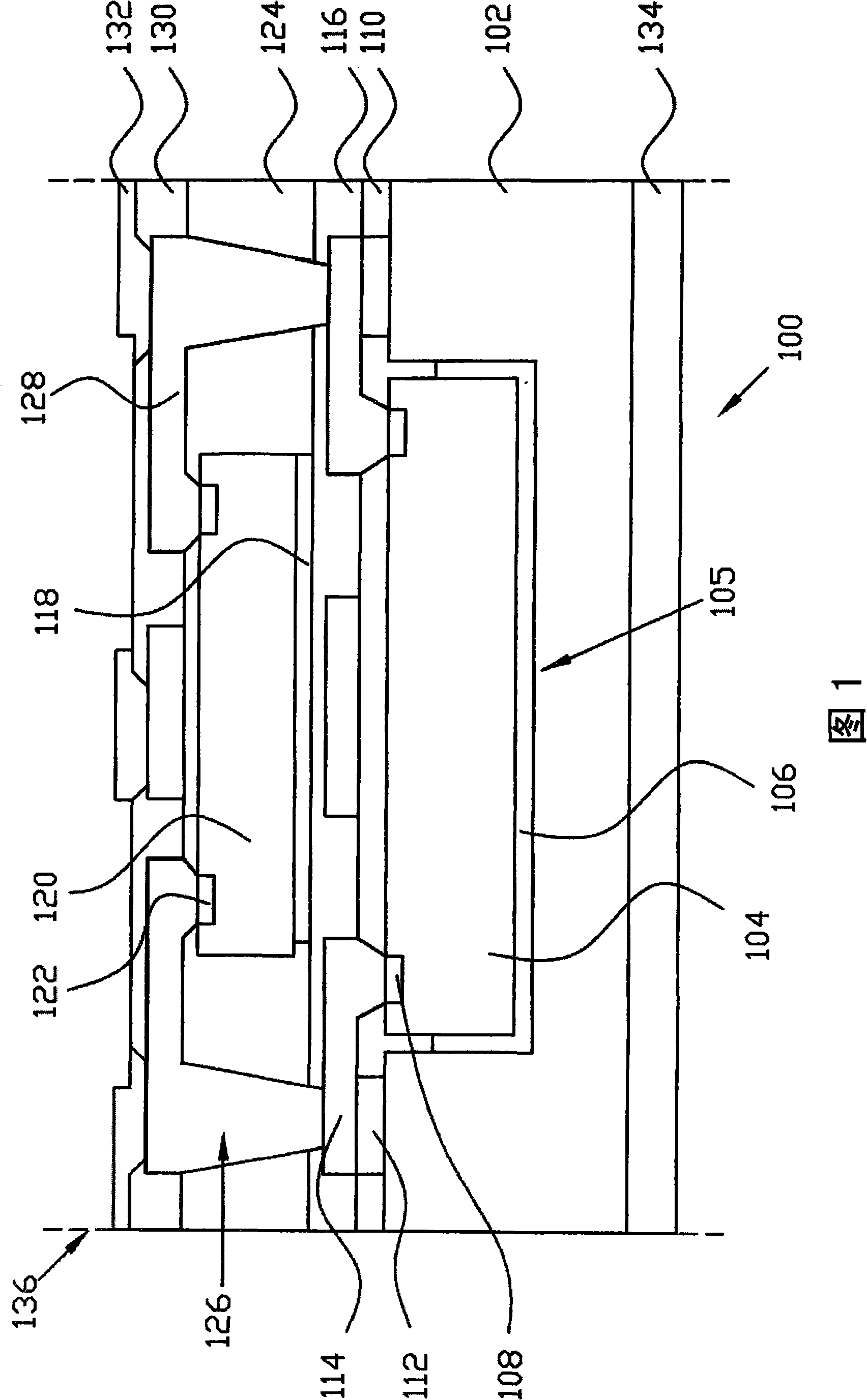
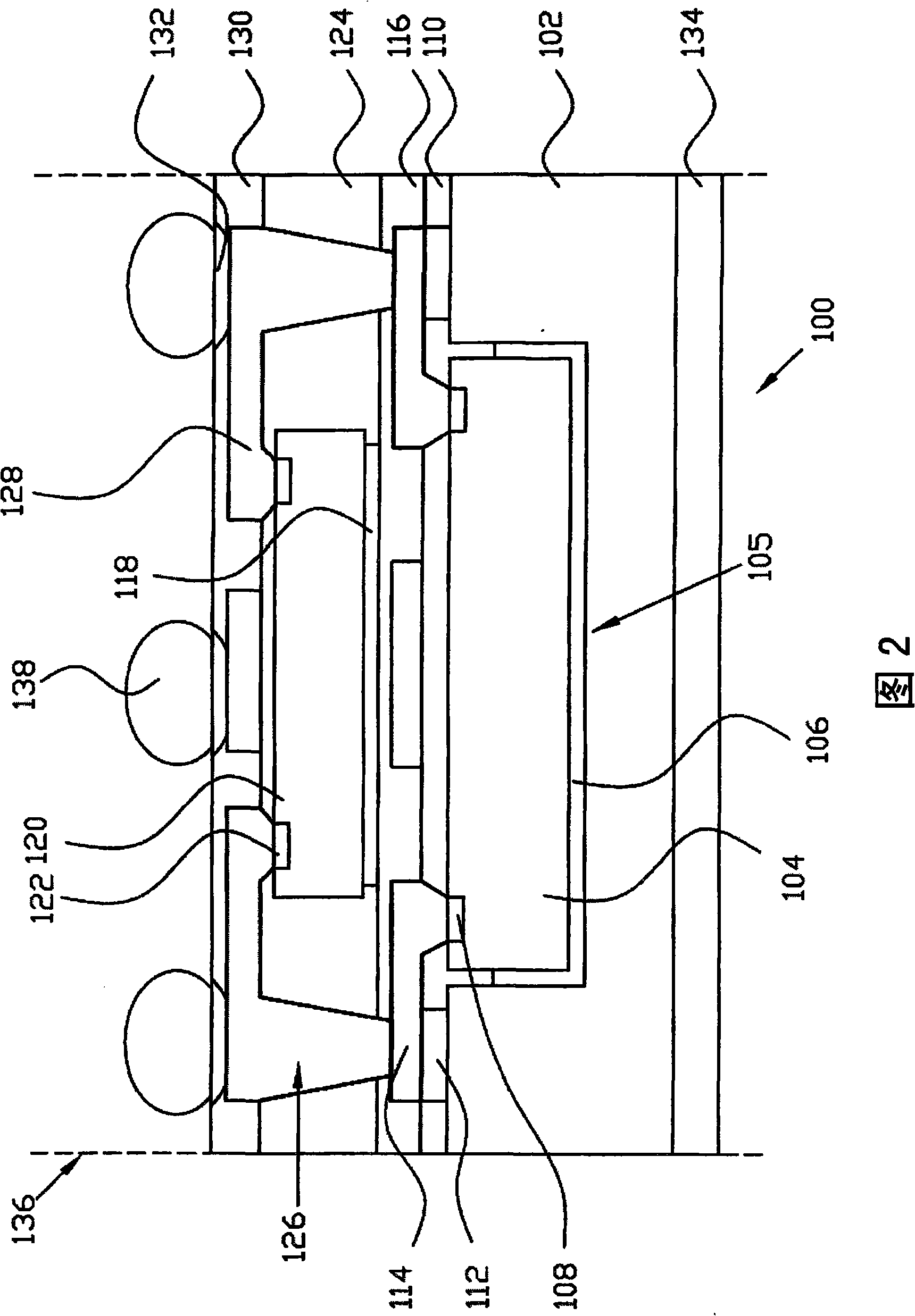
[0073] The invention discloses a packaging structure of a semiconductor component. The component utilizes a substrate with defined terminal metal pads formed thereon and a predetermined groove in the substrate. A die is disposed in the die receiving groove by adhesion. A photosensitive material is coated on the die and the preformed substrate. Preferably, the photosensitive material is made of elastic material.

[0074] Referring to FIG. 1 , it is a cross-sectional view of a semiconductor device package according to the present invention. The semiconductor device package 100 includes: a substrate 102; a first die 104; a second die 120; a die receiving groove 105; a first die attach material 106; a second die attach material 118; a first dielectric layer 110, a second dielectric layer 116 and a third dielectric layer 130; adhesive paste 124; a through hole 126; a first redistribution layer 114; a second redistribution layer 128 ; a cover layer 134 ; terminal pad 132 ; and a ...


PUM


Abstract

The present invention provides a semiconductor device package comprising a substrate with at lease a pre-formed die receiving cavity formed and terminal contact metal pads formed within an upper surface of the substrate. At lease a first die is disposed within the die receiving cavity. A first dielectric layer is formed on the first die and the substrate and refilled into a gap between the first die and the substrate to absorb thermal mechanical stress there between. A first re-distribution layer (RDL) is formed on the first dielectric layer and coupled to the first die. A second dielectric layer is formed on the first RDL, and then a second die is disposed on the second dielectric layer and surrounded by core pastes having through holes thereon. A second re-distribution layer (RDL) is formed on the core pastes to fill the through holes, and then a third dielectric layer formed on the second RDL.

Description

technical field [0001] The present invention relates to a semiconductor component packaging structure, in particular to a semiconductor component polycrystalline packaging structure with good thermal expansion coefficient matching (good CTE matching) and a method thereof. Die shifting and warpage problems to simplify the process. Background technique [0002] In recent years, the high-tech electronics manufacturing industry has introduced more functional and user-friendly electronic products. The rapid development of semiconductor technology has led to many advances, such as the reduction of semiconductor package size, the adoption of multi-pin, the adoption of fine pitch, and the miniaturization of electronic components. The purpose and advantages of Wafer Level Package (WLP) include reducing manufacturing cost, reducing the parasitic capacitance (parasitic capacitance) and parasitic inductance (parasitic inductance) effects generated by shorter conductive line paths, And...

Claims


Application Information

Patent Timeline
Patent Type & Authority Applications(China)
IPC IPC(8): H01L25/00H01L25/065H01L23/48H01L21/50H01L21/60
CPCH01L2924/01015H01L2224/24227H01L2924/15153H01L2225/06524H01L2924/01082H01L2924/15788H01L2224/97H01L2924/12041H01L2224/32245H01L2924/30105H01L2924/09701H01L24/82H01L2924/15311H01L24/19H01L23/5389H01L2924/01029H01L2924/01027H01L24/24H01L2924/01087H01L2924/014H01L25/0652H01L2924/01013H01L2924/30107H01L2224/32225H01L24/97H01L2924/15787H01L2924/157H01L2924/19043H01L2924/01047H01L2224/73267H01L2924/01079H01L2924/01068H01L25/0657H01L25/0655H01L2924/14H01L2924/01033H01L2924/01005H01L2924/01006H01L2224/24137H01L2924/15165H01L2924/01059H01L2924/01078H01L2924/10253H01L25/50H01L2924/01075H01L2224/12105H01L2924/351H01L2924/181H01L2224/05026H01L2224/05548H01L2224/05001H01L2924/00014H01L2224/02379H01L2224/82H01L2924/00H01L2224/05599H01L2224/05099H01L23/48
Inventor 杨文焜许献文
Owner ADVANCED CHIP ENG TECH INC
Why Eureka
Try Eureka