Frequency jitter implementation method and frequency jitter circuit

A technology of frequency jitter and realization method, applied in the direction of output power conversion device, electrical components, etc., can solve the problems of reducing power supply efficiency, increasing the difficulty of transformer winding and increasing high-frequency switching loss with anti-interference technology, and achieving a simple control method. Effective, simple method, and the effect of reducing circuit area

Inactive Publication Date: 2008-09-10
SUZHOU POWERON IC DESIGN
View PDF0 Cites 19 Cited by
  • Summary
  • Abstract
  • Description
  • Claims
  • Application Information

AI Technical Summary

Problems solved by technology

These methods can effectively suppress electromagnetic interference, but each method has its limitations: the use of common-mode inductors, X1 and Y1 capacitors are restricted by volume and cost; transformer anti-interference technology increases the difficulty of winding transformers, and insulation also requires Be very careful; adding a Snubber circuit to the high-frequency switch will reduce the efficiency of the power supply and increase the loss of the high-frequency switch; PCB design requires rich experience, and the convenience of product manufacturing must be considered

Method used


Image

  • Frequency jitter implementation method and frequency jitter circuit
  • Frequency jitter implementation method and frequency jitter circuit
  • Frequency jitter implementation method and frequency jitter circuit

Examples


Embodiment Construction

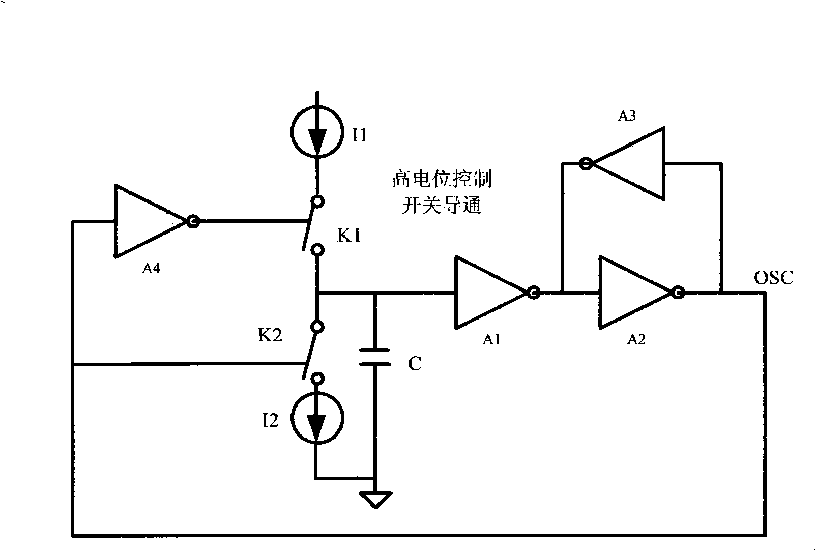
[0017] like figure 1 Shown is a circuit structure diagram of a common oscillator realized by charging and discharging a capacitor. Its working principle is as follows: At the beginning, the switch K1 is closed and K2 is opened, and the capacitor C is charged by the fixed current I1. After a period of time, the voltage on the capacitor C reaches the opening voltage of the inverter A1, the inverter A1 is turned on, and the inverter A2 is turned on. When the signal OSC is turned off, the signal OSC is at a high potential, and the inverter A3 is turned on, so that the voltage at the input terminal of the inverter A2 increases. The output signal OSC of the oscillator is high potential, the inverter turns on A4, the switch K1 opens and K2 closes, so the capacitor C starts to discharge through the fixed current I2, and the voltage on the capacitor C drops to the shutdown threshold of the inverter A1 after a period of time , the inverter A2 is turned on, and the signal OSC becomes a ...


PUM


Abstract

The invention discloses a realizing method of frequency jitter. The method is characterized in that a frequency jitter control circuit is connected in parallel with the two ends of a charging and discharging capacitor inside a vibrator to periodically change the frequency of the output of square wave by the vibrator and the frequency jitter control circuit controlled by feedback control of the output signal of the vibrator provides the capacitor with the capacitance changing periodically. The invention also discloses a frequency jitter circuit for implementing the method. By adopting the feedback control of the output signal of the vibrator to form the frequency jitter, the method spares the external frequency source and is simple and saves cost and reduces the circuit area; the frequency jitter control circuit of the invention is simple and easy to be integrated; the control of the method is simple and effective and can eliminate misoperation caused by the delay of a gate circuit by adopting a binary synchronous counter to receive the output signal of the vibrator and with the counting function thereof forming the feedback control signal through parallel data output terminals.

Description

technical field [0001] The invention relates to a method for realizing internal oscillator frequency jitter in a switching power supply integrated circuit and a frequency jitter circuit. Background technique [0002] Compared with the traditional linear regulated power supply, the switching power supply does not require a large-scale power transformer, and has the characteristics of small size, light weight, high efficiency, low standby power consumption, and wide voltage regulation range. It is widely used in household appliances, automatic control , communications, computers and other fields. However, the electromagnetic interference signal generated by the switching power supply itself occupies a wide frequency band and a strong amplitude. If it is not properly controlled, it will generate electromagnetic interference to surrounding equipment through conduction and radiation, pollute the electromagnetic environment, and become a strong source of electromagnetic interferen...

Claims


Application Information

Patent Timeline
Patent Type & Authority Applications(China)
IPC IPC(8): H02M1/00H02M1/08
Inventor 易扬波陶平王钦
Owner SUZHOU POWERON IC DESIGN
Why Eureka
Try Eureka