Quantum point-trap infrared detector structure and method for producing the same

A technology of infrared detectors and quantum dots, applied in semiconductor devices, final product manufacturing, sustainable manufacturing/processing, etc., can solve problems such as low quantum efficiency of devices, large dark current, and increased costs

Inactive Publication Date: 2008-09-24
INST OF SEMICONDUCTORS - CHINESE ACAD OF SCI
View PDF0 Cites 14 Cited by
  • Summary
  • Abstract
  • Description
  • Claims
  • Application Information

AI Technical Summary

Problems solved by technology

[0003] (1) The quantum efficiency of the device is low
[0004] (2) Due to the polarization selectivity of QWIP infrared absorption, it has to introduce grating coupling, which greatly increases the complexity of QDIP production and increases the cost
However, due to the randomness of quantum dot growth, it is

Method used


Image

  • Quantum point-trap infrared detector structure and method for producing the same

Examples


Embodiment Construction
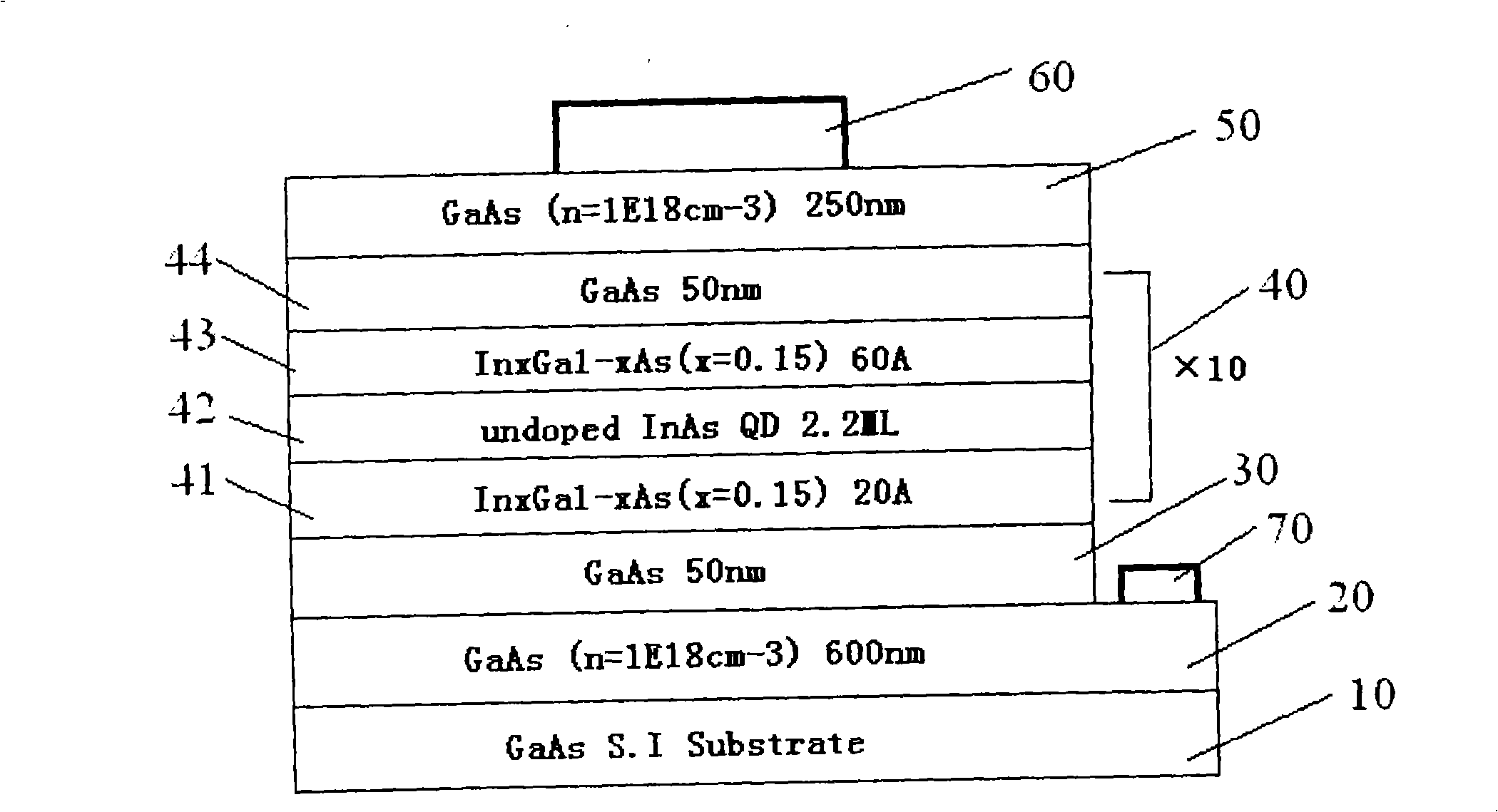
[0045] figure 1 It is the core idea of ​​the present invention, that is, it is used in the growth process of the quantum dot-well structure infrared detector.

[0046] (1) First grow a highly doped GaAs bottom contact layer 20 on a semi-insulating GaAs substrate 10; the doping element is Si, and the doping concentration is 1×10¹⁸ / cm 3, the growth temperature is 580°C, and the thickness is 600nm. The purpose of doping the GaAs bottom contact layer 20 with a high concentration is to form a good ohmic contact with the electrode material AuGe / Ni / Au instead of a Schottky contact when the lower electrode 70 is fabricated later. The relatively thick 600nm growth is to facilitate the etching operation in the subsequent device manufacturing process;

[0047] (2) Then grow an undoped lower GaAs spacer layer 30 on the highly doped GaAs bottom contact layer 20 at a growth temperature of 580° C. and a thickness of 50 nm. The purpose of growing the undoped lower GaAs isolation layer 30 i...


PUM

PropertyMeasurementUnit
Thicknessaaaaaaaaaa
Thicknessaaaaaaaaaa
Thicknessaaaaaaaaaa

Abstract

A quantum dot-trap infrared receiver structure includes: a semi-insulating GaAs underlay, a GaAs bottom contact layer which is made on the semi-insulating GaAs underlay, a lower GaAs isolation layer which is made at one side of the GaAs bottom contact layer, and a table-board is formed at the other side of the GaAs bottom contact layer; an InAs/InGaAs dot-trap structure layer with 10 periods is made on the lower GaAs isolation layer and is the core part in which photocurrent is formed and the infrared detection is finally realized; a GaAs top contact layer is made on the InAs/InGaAs dot-trap structure layer with 10 periods; an upper electrode is made on the middle part of the GaAs top contact layer, and the externally added voltages carried on the detector can be realized by the upper electrode; the lower electrode is made on the table-board of the GaAs top contact layer, and the externally added voltages carried on the detector can be realized by the lower electrode.

Description

technical field [0001] The invention relates to semiconductor technology, mainly growing an InAs / InGaAs point-well structure used for a quantum dot infrared detector on a semi-insulating GaAs substrate, in particular to a structure of a quantum dot-well infrared detector and a preparation method thereof . Background technique [0002] As an advanced technology, middle and far infrared detection is widely used in military and national economic construction. At present, the commonly used mid-to-far infrared detectors mainly include HgCdTe infrared detector (MCT) and quantum well infrared detector (QWIP), but they all have their own problems that are difficult to solve. For MCT, it is not only difficult to grow uniform large-area materials for focal plane array (FPA) and uniform doping, which makes the imaging quality of MCT focal plane poor, but also needs to be achieved at a temperature less than or equal to 80K. Infrared detection. In addition, it also has a relatively la...

Claims


Application Information

Patent Timeline
IPC IPC(8): H01L31/08H01L31/09H01L31/101H01L31/18
CPCY02P70/50
Inventor 王志成徐波刘峰奇陈涌海王占国石礼伟梁凌燕
Owner INST OF SEMICONDUCTORS - CHINESE ACAD OF SCI
Why Eureka
Try Eureka