An electronic emitter on silicon-based surface and preparation method thereof

A surface electron and emission device technology, applied in the manufacture of semiconductor/solid-state devices, electrical components, electrode systems, etc., can solve the problems of complex manufacturing process, limited development of field emission displays, unsatisfactory emission stability and service life, etc.

Inactive Publication Date: 2008-10-15
ZHEJIANG UNIV
View PDF0 Cites 10 Cited by
  • Summary
  • Abstract
  • Description
  • Claims
  • Application Information

AI Technical Summary

Problems solved by technology

However, in electron-emitting devices, the manufacturing process of commonly used tapered emitter arrays and carbon nanotubes in the research stage are

Method used


Image

  • An electronic emitter on silicon-based surface and preparation method thereof
  • An electronic emitter on silicon-based surface and preparation method thereof

Examples


Embodiment 1

[0020] Take the following process steps:

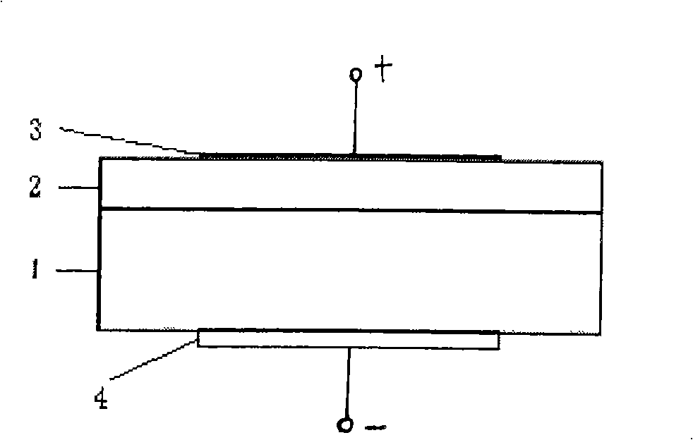
[0021] 1) Clean n-type , resistivity 0.005 ohm cm, size 15×15mm 2 , a silicon wafer with a thickness of 675 microns;

[0022] 2) Heat the silicon wafer at 900°C for 2 hours in an oxygen atmosphere to obtain SiO with a thickness of 30nm 2 film;

[0023] 3) On SiO 2 A 20nm thick Au film was sputtered on the thin film as a gate, and a 100nm thick Au film was sputtered on the back of the silicon substrate as an ohmic contact electrode.

Embodiment 2

[0025] Take the following process steps:

[0026] 1) Clean n-type , resistivity 0.5 ohm cm, size 15×15mm 2 , a silicon wafer with a thickness of 675 microns;

[0027] 2) With tetraethyl orthosilicate (TEOS) as the gas source, SiO with a thickness of 100 nm was deposited on the silicon wafer by chemical vapor deposition. 2 thin film, the deposition temperature is 500°C, and the working pressure is 100Torr;

[0028] 3) On SiO 2 A 20nm thick Al film was sputtered on the thin film as a gate, and a 100nm thick Au film was sputtered on the back of the silicon substrate as an ohmic contact electrode.

Embodiment 3

[0030] Take the following process steps:

[0031] 1) Clean n-type , the resistivity is 50 ohm cm, the size is 15×15mm 2 , a silicon wafer with a thickness of 675 microns;

[0032] 2) Using sapphire particles as the evaporation source, deposit Al with a thickness of 100nm on the silicon wafer by electron beam evaporation method 2 o 3 film;

[0033] 3) in Al 2 o 3 A 30nm thick Au film was sputtered on the thin film as a gate, and a 100nm thick Au film was sputtered on the back of the silicon substrate as an ohmic contact electrode.


PUM

PropertyMeasurementUnit
Thicknessaaaaaaaaaa
Thicknessaaaaaaaaaa

Abstract

The invention discloses a silica-based surface electronic emitter and a preparation method thereof. The emitter deposits a SiO2 or Al2O3 thin film layer at the front of an 'n' type silicon substrate, a gate electrode is deposited on the SiO2 or Al2O3 thin film layer and an ohmic contact electrode is deposited at the back of the silicon substrate; the producing method comprises the following steps: an 'n' type silicon chip is washed firstly; a SiO2 or Al2O3 thin film is deposited on the silicon chip by a thermal oxidation method or a chemical vaporous deposition method or an evaporation method or a sputtering method or a sol-gel method; the gate electrode is sputtered on the SiO2 or Al2O3 thin film, and the ohmic contact electrode is sputtered at the back of the silicon substrate. The silica-based surface electronic emitter of the invention has higher electronic emission energy and good performance for high field emission, can be used for producing a field emission display, has simple producing technique and is compatible with the existing mature silicon device planar technique.

Description

technical field [0001] The invention relates to a silicon-based surface electron emission device and a preparation method thereof. Background technique [0002] In 1961, K.R.Shoulders proposed the idea of ​​a microelectronic device based on a field emission cathode array; in 1968, C.Spindt developed a field emission cathode array for the first time; until 1985, A.Ghis et al. of France LETI used a field emission cathode array Emit electrons to excite phosphors to prepare the first field emission display, which triggered a research boom in field emission displays (references: K.R.Shoulders, Adv.Comput.2, 135(1961); C.A.Spindt, J.Appl.Phys 39, 3504 (1968); A. Ghis et. al., IEEE Trans. Electron. 38, 2320 (1993)). Field emission displays inherit the advantages of traditional cathode ray tube displays in terms of brightness, grayscale, color, resolution and response speed. In addition, field emission displays also have thin, low power consumption, self-illumination, low operating...

Claims


Application Information

Patent Timeline
IPC IPC(8): H01J1/316H01J1/30H01J9/02H01J29/02H01J29/04H01J31/12H01L21/00
Inventor 陈培良马向阳李东升杨德仁
Owner ZHEJIANG UNIV
Why Eureka
Try Eureka