Fractal photon band-gap folding line microstrip antenna for ultra-broadband system

A technology of photonic bandgap and microstrip antenna, applied in the direction of antenna, resonant antenna, radiating element structure and other directions, to achieve the effect of large bandwidth, simple manufacturing process and simple structure

Inactive Publication Date: 2008-11-12
XIAMEN UNIV
View PDF0 Cites 3 Cited by
  • Summary
  • Abstract
  • Description
  • Claims
  • Application Information

AI Technical Summary

Problems solved by technology

At present, there is no report on the related technology of combining the meander line microstrip antenna with the fractal PBG structure and applying it in the ultra-wideband communication frequency band of 3.1-10.6GHz

Method used


Image

  • Fractal photon band-gap folding line microstrip antenna for ultra-broadband system
  • Fractal photon band-gap folding line microstrip antenna for ultra-broadband system
  • Fractal photon band-gap folding line microstrip antenna for ultra-broadband system

Examples


Embodiment Construction

[0030] The present invention will be further described below in conjunction with the embodiments and the drawings.

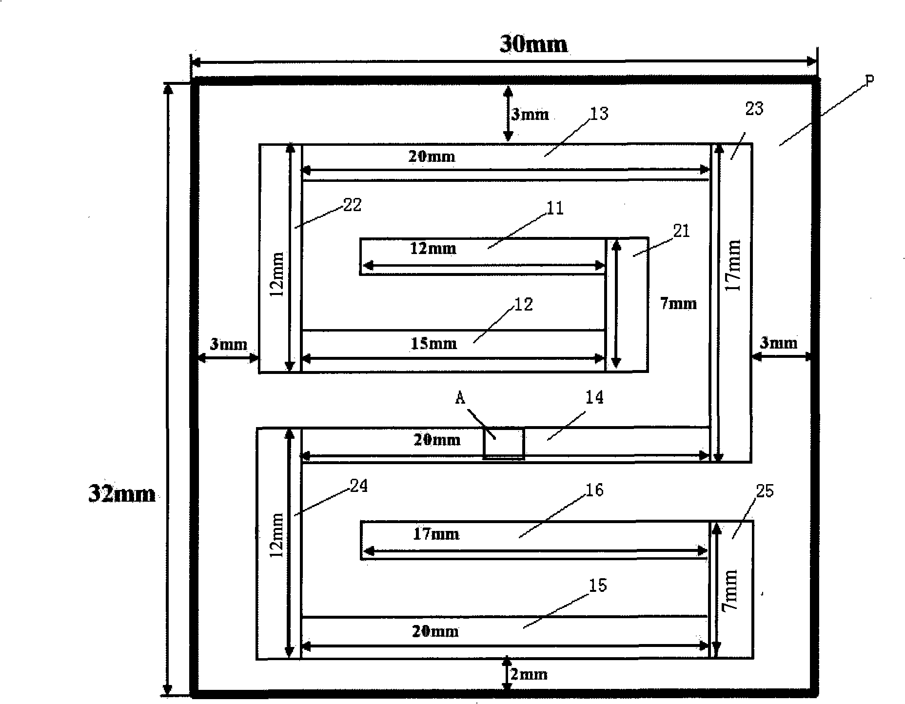
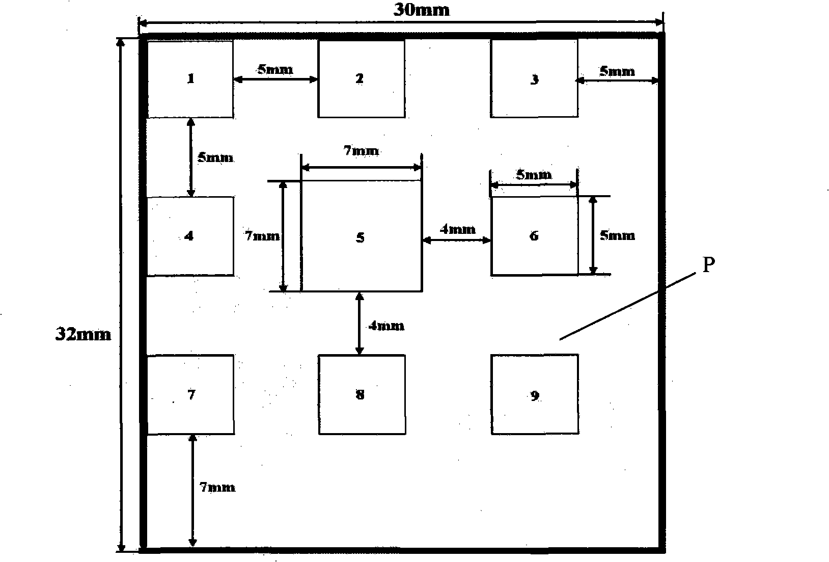
[0031] See figure 1 with figure 2 , The present invention is provided with a double-sided copper-clad dielectric substrate P, the dielectric substrate P is a rectangular dielectric substrate, and its size is 30 mm in length, 32 mm in width, and 1 mm in thickness. The dielectric substrate P uses a dielectric substrate with a relative dielectric constant of 2.25±5%. The dielectric substrate P uses an epoxy resin glass cloth dielectric substrate, and the copper layer on one side of the dielectric substrate P is a bending line microstrip antenna radiation patch (such as figure 1 As shown), the copper-clad layer on the other side of the dielectric substrate P has a fractal photonic band gap structure (such as figure 1 Shown).

[0032] The bending line microstrip antenna radiation patch is provided with 6 transverse arms (11, 12, 13, 14, 15 and 16) and 5 longitudinal ...


PUM


Abstract

The invention discloses a fractal photon band gap meander-line microstrip antenna used for an ultra-wideband system, which relates to a microstrip antenna, and provides the fractal photon band gap meander-line microstrip antenna which has small dimension, wide bandwidth, and lower return loss, is provided with an omni-directional radiation characteristic, and is used for the ultra-wideband system. The antenna of the invention is provided with a dielectric substrate with copper bonded layers at two sides; the copper bonded layer at one side of the dielectric substrate is a meander-line microstrip antenna radiating patch, while the copper bonded layer at the other side of the dielectric substrate is a fractal photon band gap structure; the meander-line microstrip antenna radiating patch is provided with at least 4 transverse arms and at least 3 vertical arms, the ends of each transverse arm and each vertical arm are alternately connected in series, and the two ends of each vertical arm are respectively connected with the one end of two transverse arms and are in a U shape; the fractal photon band gap structure is provided with a total of 9 copper sheets which are arranged in 3 lines and 3 columns, each line is provided with 3 copper sheets which are distributed at intervals, and each column is provided with 3 copper sheets which are distributed at intervals; the lines are mutually in parallel, while the columns are also mutually in parallel, the copper sheets in each line are in parallel, and the copper sheets in each column are in parallel.

Description

Technical field [0001] The invention relates to a microstrip antenna, in particular to a fractal photonic band gap (PBG) bent line microstrip antenna used in an ultra-wideband system. Background technique [0002] In 2002, the US Federal Communications Commission (FCC) announced that the frequency band for ultra-wideband (UWB) communications was defined as 3.1~10.6GHz. This frequency band can be used for wireless local area network (WPAN), as well as for precise ranging, metal detection, etc. use. After the IEEE802.15.3a standard was proposed, the ultra-wideband wireless access technology was further standardized. Ultra-wideband technology has attracted much attention because of its low cost, high data transmission rate, penetrability, and low transmit power. It has become a major research hotspot in wireless communications. [0003] Antenna design and manufacturing technology is one of the core key technologies of the ultra-wideband communication system. The characteristics and ...

Claims


Application Information

Patent Timeline
Patent Type & Authority Applications(China)
IPC IPC(8): H01Q1/38H01Q9/04H01Q13/08
Inventor 游佰强林斌付尧周建华徐伟明施芝元刘舜奎李伟文
Owner XIAMEN UNIV
Why Eureka
Try Eureka