Transparent semiconductor film diode and preparing method thereof

A thin-film diode and transparent thin-film technology, applied in the field of transparent semiconductor thin-film diodes and their preparation, can solve the problems that transparent electronic devices are in the laboratory stage and not commercialized.

Inactive Publication Date: 2008-11-19
FUDAN UNIV
View PDF0 Cites 2 Cited by
  • Summary
  • Abstract
  • Description
  • Claims
  • Application Information

AI Technical Summary

Problems solved by technology

However, due to the interface effects of different thin films and the compatibility differences between the preparation processes, most of the existing research on transparent electronic devices is still in the laboratory stage and has not been commercialized.

Method used


Image

  • Transparent semiconductor film diode and preparing method thereof
  • Transparent semiconductor film diode and preparing method thereof
  • Transparent semiconductor film diode and preparing method thereof

Examples


Embodiment 1

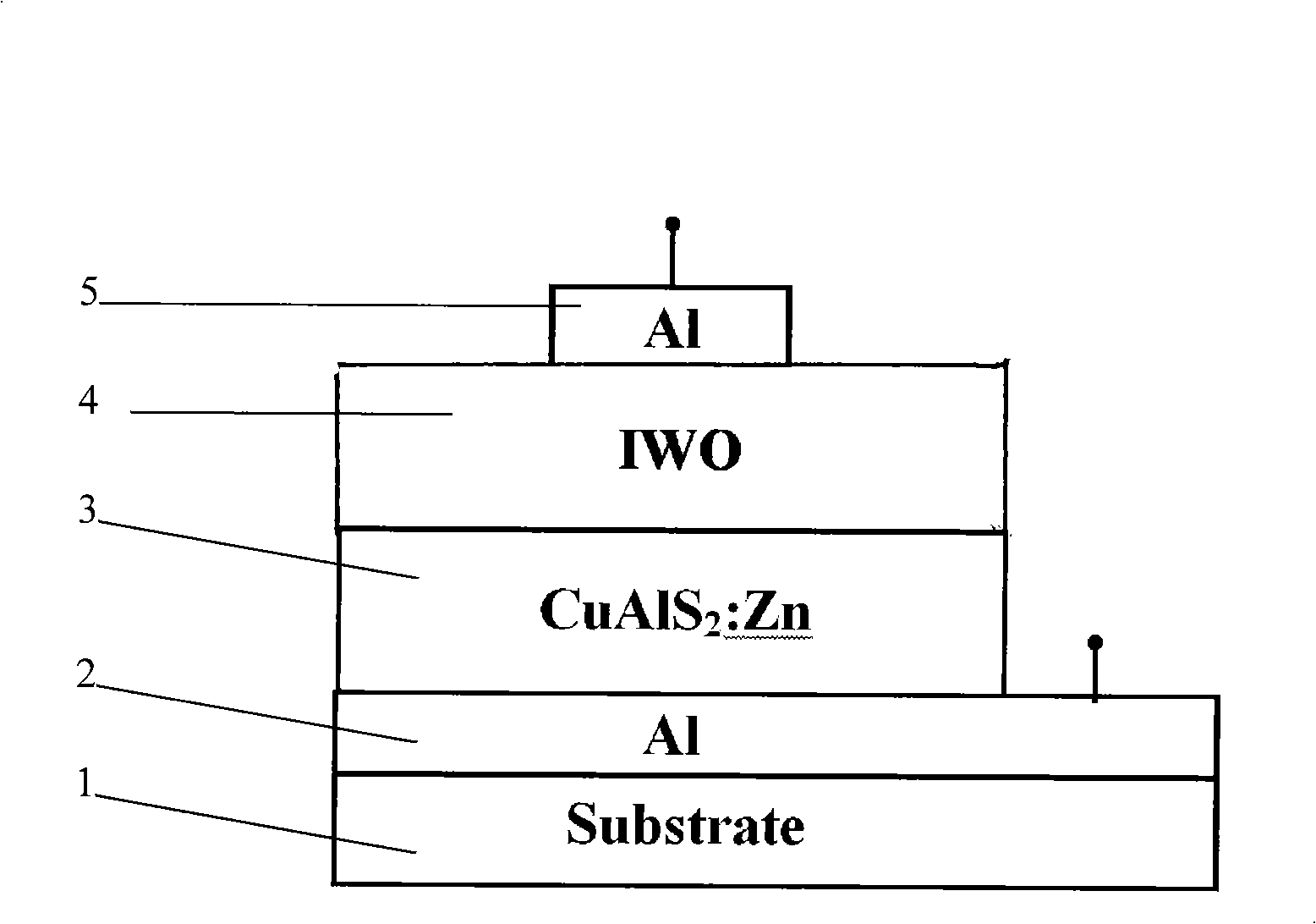
[0018] Embodiment 1, the first step, using the pulsed plasma deposition method to deposit p-type conductive CuAl on a common glass substrate 0.90 Zn 0.10 S 2 film. Preparation of CuAl according to traditional ceramic target preparation method 0.90 Zn 0.10 S 2 Circular target with a target diameter of 15 mm. The distance between the target surface and the quartz tube was fixed at 4 mm. The inner diameter of the quartz catheter is 2mm. The substrate is a common glass slide, which is ultrasonically cleaned with deionized water, acetone and alcohol for 20 minutes each. The background pressure of the vacuum chamber before film deposition was 2.0×10 -4 Pa.

[0019] Use the gas flow meter of Bronkhorst Company to control the flow of Ar so that the pressure of the working gas is 2.4Pa, the temperature of the substrate is kept at room temperature, and the voltage and current of the ablation source are set to -18.0KV and 4.2 mA, the pulse electron beam repetition frequency is ...

Embodiment 2

[0021] Embodiment 2, the same step and method as embodiment 1, only in the preparation of CuZn 0.1 al 0.9 S 2 Change the preparation parameters when thin film: the ablation gas pressure is 2.4Pa, the substrate temperature is still at room temperature, the ablation source voltage and current are set to -18.0KV and 4.2mA respectively in the power supply, and the pulse electron beam repetition frequency is 2.0Hz. The film deposition time is 60 minutes, and the film thickness is 70 nm.

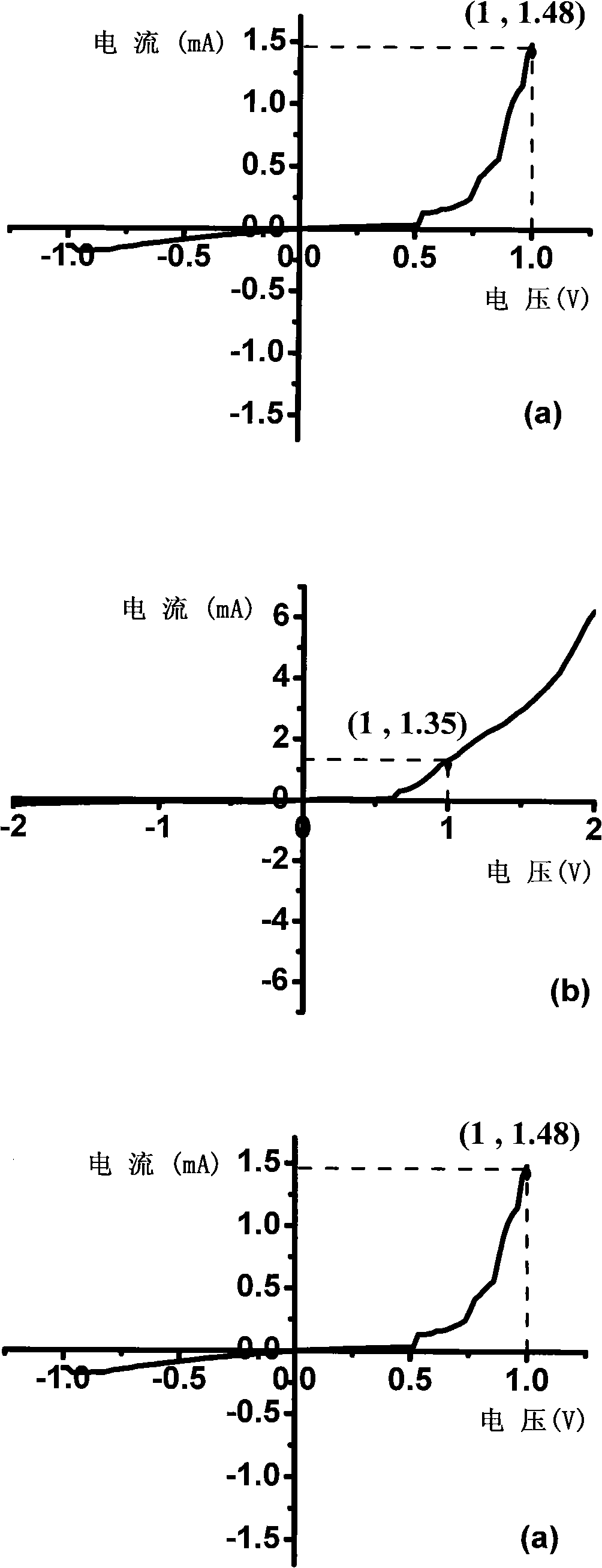
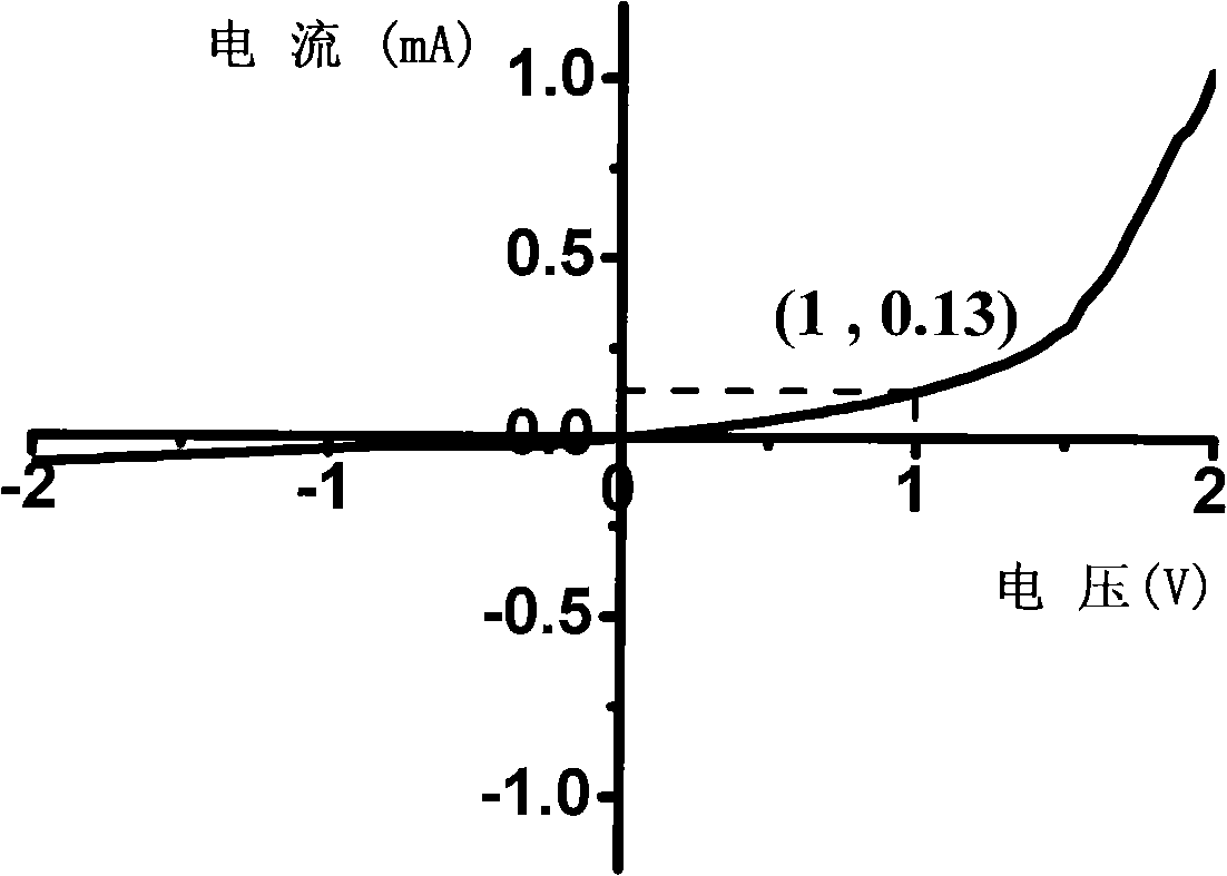
[0022] The thickness of each layer of film was measured with a Kosaka ET3000 surface profiler. The sheet resistance of each film at room temperature was measured using a BD-90 four-probe instrument. The Seebeck coefficient and Hall coefficient of the film were measured at room temperature using a Hall test system (Accent HL5500 Hall System). The transmission spectrum of the transparent device in the visible light range was measured with a Shimadzu UV2450 ultraviolet / visible spectrophotometer. ...


PUM

PropertyMeasurementUnit
thicknessaaaaaaaaaa
thicknessaaaaaaaaaa
thicknessaaaaaaaaaa

Abstract

The invention relates to transparent electronics field and in particular relates to a transparent semiconductor film diode and a fabrication method thereof. The transparent semiconductor film diode is made by combining a p type CuALS2:Zn transparent semiconductor film with a n type In2O3:W transparent semiconductor film, thus forming a CuALS2:Zn-In2O3:W transparent semiconductor film transistor. The invention takes normal glass as the substrate, and firstly, a type CuALS2: Z film is developed through pulse plasma sedimentation plating; then a n type In2O3:W film is developed on the CuALS2:Zn film through direct magnetic control sputtering under room temperature. The film diode has good rectifying property and good transparency, thus forming a new heterojunction transparent semiconductor film diode. The transparent semiconductor film diode is of good application prospect in the field of optoelectronic devices.

Description

technical field [0001] The invention belongs to the technical field of transparent electronics, and in particular relates to a transparent semiconductor thin film diode and a preparation method thereof. Background technique [0002] The combination of the new p-type conductive transparent film and the existing n-type transparent conductive oxide (TCO) film can realize transparent electronic devices such as transparent diodes and transparent thin film transistors, forming a new discipline-transparent electronics. The emergence of transparent electronics not only enriches and develops the connotation of silicon-based electronics, but also has a wide range of application values ​​in the fields of solar cells, flat panel displays, and photodetectors. [0003] In 1997, Kawazoe et al. reported CuAlO 2 Since it has p-type conductivity and transparency in the visible region, many new p-type conductive transparent semiconductor thin film materials have emerged, and their photoelectr...

Claims


Application Information

Patent Timeline
Patent Type & Authority Applications(China)
IPC IPC(8): H01L29/861H01L29/267H01L21/329C23C14/06C23C14/08C23C14/54
Inventor 张群王颖华施展
Owner FUDAN UNIV
Why Eureka
Try Eureka