Weak-brightness non-crystal silicon solar cell manufacture method using laser etching transparent electrode

A solar cell and transparent electrode technology, applied in the field of solar cells, can solve the problems of increasing waste comprehensive treatment expenditure, affecting product electrical performance, and consuming more raw materials, so as to improve product yield, simplify production process, and reduce raw material loss. Effect

Inactive Publication Date: 2008-11-19
PUTIAN WEITE ELECTRONICS
View PDF0 Cites 9 Cited by
  • Summary
  • Abstract
  • Description
  • Claims
  • Application Information

AI Technical Summary

Problems solved by technology

This method of producing low-light amorphous silicon solar cells by silk-screen etching transparent electrodes consumes more raw materials, increases the cost of comprehensive treatment of waste, an

Method used


Image

  • Weak-brightness non-crystal silicon solar cell manufacture method using laser etching transparent electrode
  • Weak-brightness non-crystal silicon solar cell manufacture method using laser etching transparent electrode
  • Weak-brightness non-crystal silicon solar cell manufacture method using laser etching transparent electrode

Examples


Embodiment 1

[0024] The present invention is a method for manufacturing a low-light amorphous silicon solar cell that uses a laser to mark a transparent electrode. Embodiment 1 is a method for producing an inline low-light amorphous silicon solar cell whose product model is N8527.

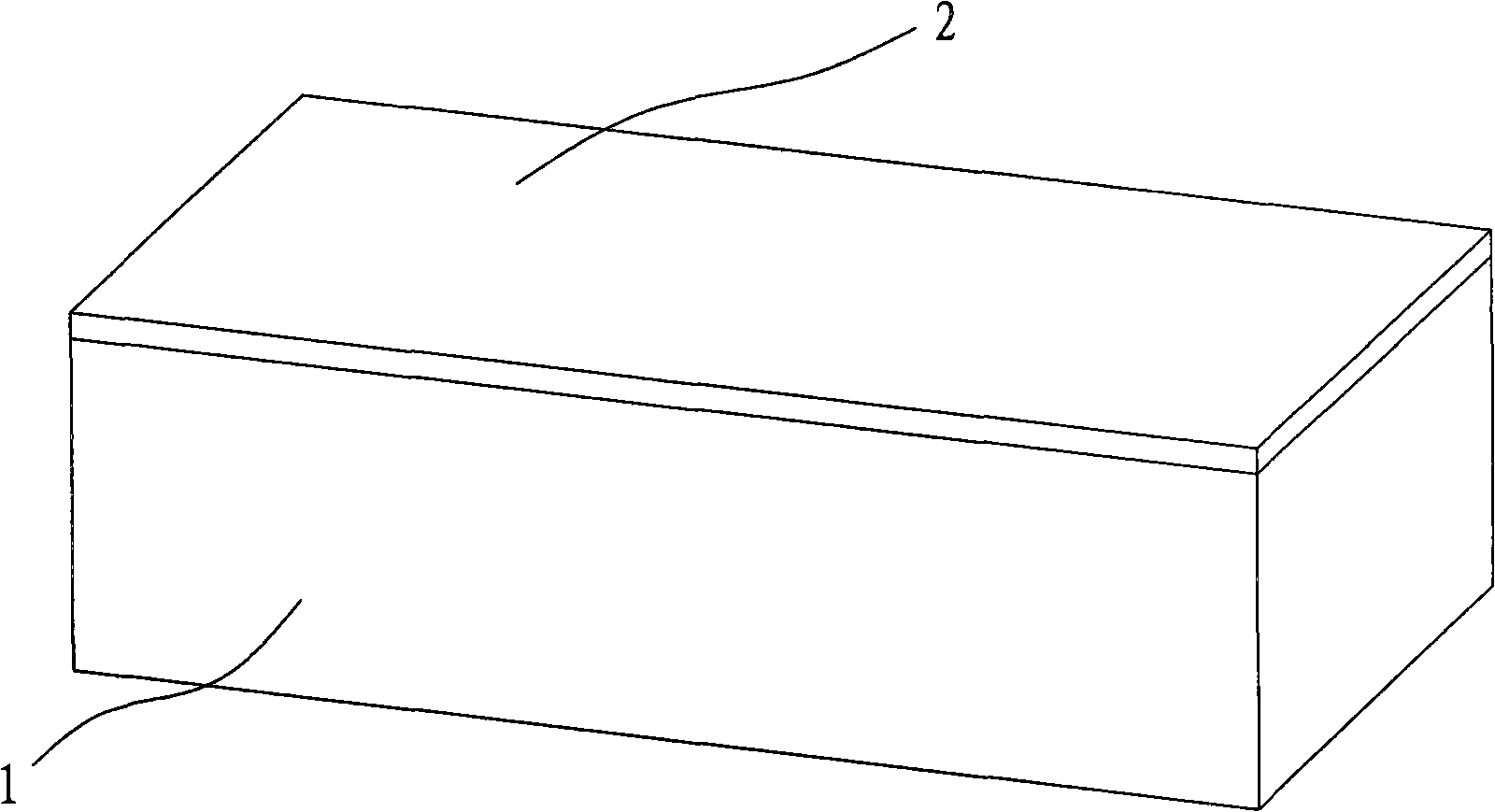
[0025] like figure 1 As shown, the conductive glass used in this embodiment includes a glass substrate 1 and an indium tin oxide transparent conductive film 2. The glass substrate 1 is an ultra-thin ITO conductive glass with a thickness of 1.1mm, and its external dimensions are 406.4mm long and 355.6mm wide. mm, thickness 1.1mm. The surface of the glass substrate 1 is sputter-deposited with a thickness of 600A 0 indium tin oxide transparent conductive film 2 .

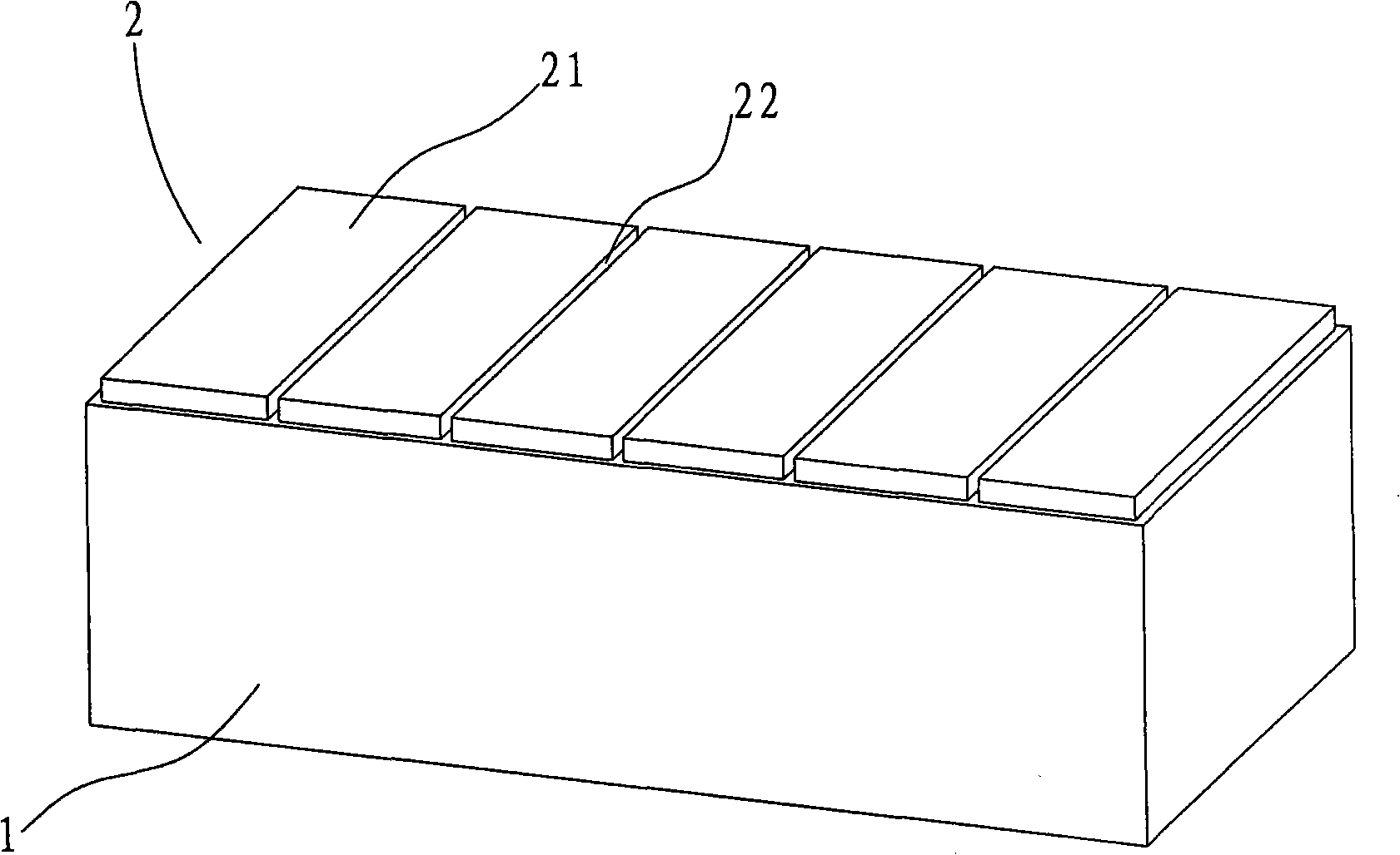
[0026] First of all, clean the conductive glass through a cleaning machine, and set it on the program of the red laser marking machine, such as figure 2 As shown, the transparent conductive film 2 of the ultra-thin ITO conductive glass is marked wit...

Embodiment 2

[0037] Embodiment 2 of the present invention is a method for producing Wailian low-light amorphous silicon solar cells whose product model is W5514.

[0038] The conductive glass in the present embodiment is still the conductive glass used in embodiment one, as figure 1 As shown, it includes a glass substrate 1 and an indium tin oxide transparent conductive film 2. The glass substrate 1 is an ultra-thin ITO conductive glass with a thickness of 1.1mm, and its dimensions are 406.4mm in length, 355.6mm in width and 1.1mm in thickness. The surface of the glass substrate 1 is sputter-deposited with a thickness of 600A 0 indium tin oxide transparent conductive film 2 .

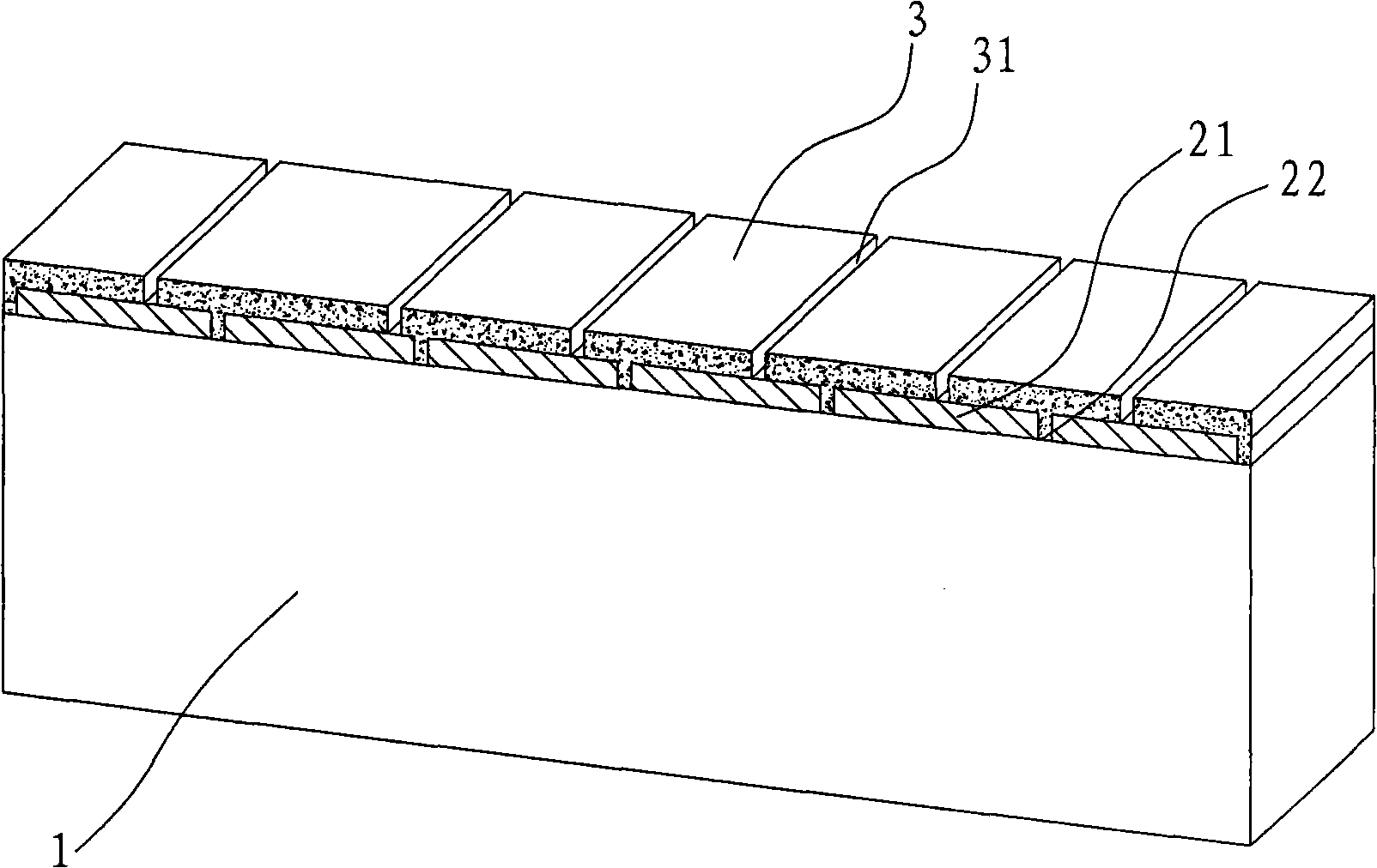
[0039] Firstly, the conductive glass is cleaned by a cleaning machine, and then, the program of the red laser marking machine is set, and the transparent conductive film 2 is marked by the red laser marking machine as shown in the following figure: Figure 5 In the five amorphous silicon solar cell transparent ele...


PUM

PropertyMeasurementUnit
Thicknessaaaaaaaaaa
Sizeaaaaaaaaaa
Thicknessaaaaaaaaaa

Abstract

The invention discloses a method to fabricate a weak light amorphous silicon solar cell, which scribes the transparent electrodes through laser. The method includes the following processes(1), transparent electrode isolation grooves are scribed on the film of an ultra-thin conductive glass through a red laser scriber so as to form insulated transparent electrodes for the amorphous silicon solar cell;(2), a P-I-N amorphous silicon layer is deposited on the surface of the ultra-thin conductive glass through vacuum plating.; (3), isolation grooves penetrating the P-I-P amorphous silicon layer are scribed on the surface of the amorphous silicon film through a green laser scriber so as to expose the transparent electrodes in the isolating grooves; (4) conductive printing ink is printed on the surface of the amorphous silicon layer through a screen printing machine so as to form insulated and isolated back electrodes which respectively penetrate the isolation grooves and are electrically connected with the corresponding transparent electrodes through the amorphous silicon layer; (5), protective lacquer, conductive copper slurry and characters are processed on the back electrodes through screen printing. The invention can not only reduce production cost but also simplify production process and is good for improving the electrical properties of the products.

Description

technical field [0001] The invention discloses a method for manufacturing a weak-light amorphous silicon solar cell by laser marking a transparent electrode, which belongs to the field of solar cells. Background technique [0002] At present, the general practice of amorphous silicon solar cell manufacturers is: (1) Clean the 600A sputtered conductive film with a cleaning machine 0 (2) screen-print acid-resistant ink on the table of the screen printing machine, (3) put it in the oven and bake it at a temperature of 120°C for 10 minutes, and then take it out after the temperature drops to 45°C (4) Etching with an acidic solution by an etching machine to obtain etched lines. The concentration of the acidic solution is 6.4-6.7mol. (5) Washing off the production process of the acid-resistant ink with an alkaline solution to obtain conductive glass with etched lines. The concentration of the alkaline solution is 1.8-2.2mol. (6) After vacuum coating, a P-I-N structure amorphous s...

Claims


Application Information

Patent Timeline
IPC IPC(8): H01L31/20
CPCY02P70/50
Inventor 佘金荣邵明戴国清
Owner PUTIAN WEITE ELECTRONICS
Why Eureka
Try Eureka