CMOS image sensor and method for forming same

An image sensor and pixel unit technology, applied in the manufacture of electric solid-state devices, semiconductor devices, semiconductor/solid-state devices, etc., can solve problems such as difficult wiring, channel length cannot be reduced, and pixel unit difficulties

Active Publication Date: 2008-11-26
SEMICON MFG INT (SHANGHAI) CORP +1
View PDF2 Cites 10 Cited by
  • Summary
  • Abstract
  • Description
  • Claims
  • Application Information

AI Technical Summary

Problems solved by technology

However, CIS designers use the widely used 0.18μm technology to design very small pixel units (pixel unit size is less than 2.8×2.8μm 2 ) is more difficult
There are two main reasons. First, as the size of the pixel unit shrinks, if the technology node is the same, the operating voltage of the pixel unit is the same, which means that the threshold voltage

Method used


Image

  • CMOS image sensor and method for forming same
  • CMOS image sensor and method for forming same
  • CMOS image sensor and method for forming same

Examples


Embodiment Construction

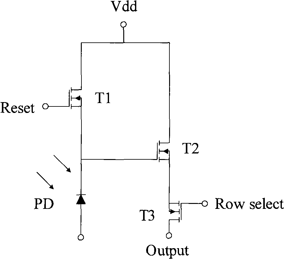
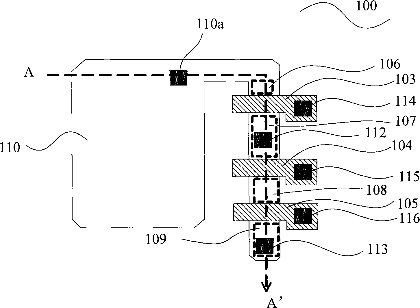
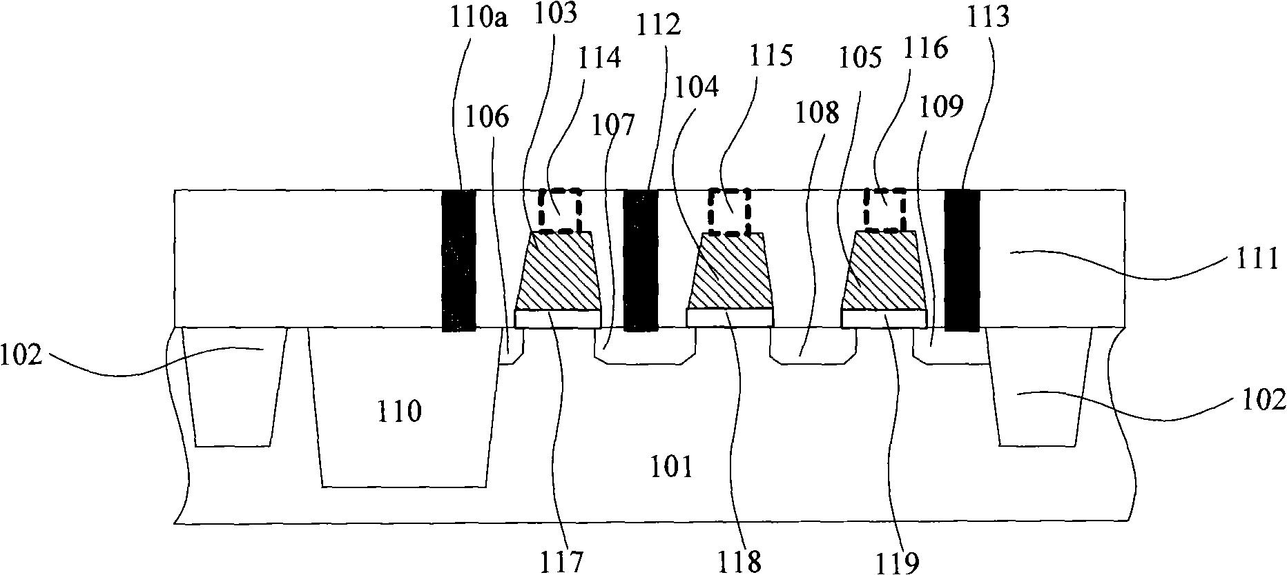
[0055] The present invention shares an output contact hole by connecting the column of the CMOS image sensor to the drains of the output transistors of the first pixel unit and the second pixel unit of the adjacent pixel unit pair; or by connecting the pixel unit pair of the CMOS image sensor The drains of the output transistors of the first pixel unit and the second pixel unit are connected to share an output contact hole, and at the same time, the drains of the reset transistors of the first pixel unit are connected to the second pixel of the adjacent CMOS image sensor pixel unit column. The drain of the reset transistor of the unit is connected to share a power contact hole, and the drain of the reset transistor of the second pixel unit is connected to the drain of the reset transistor of the first pixel unit of another adjacent CMOS image sensor pixel unit pair in the column direction. Connect and share a power contact hole. Under the condition of not lowering the technolo...


PUM


Abstract

A CMOS image sensor comprises at least one CMOS image sensor pixel unit pair which comprises a first pixel unit and a second pixel unit. Each pixel unit in the CMOS image sensor comprises a photodiode area and a drive circuit area, wherein the drive circuit area comprises output transistors. Drain electrodes of the two output transistors adjacent to the first pixel unit and the second pixel unit are connected to be a common output end. The invention further provides another CMOS image sensor, wherein the amount of effective contact holes can be reduced through an output contact hole and a power contact hole of a common output transistor of the adjacent pixel units, thereby effectively decreasing the amount of the contact holes. The structure enables pixel units with smaller dimension to be designed under the condition of unreduced technical nodes without modifying a peripheral circuit and the processing parameter, which can not increase the mask and processing cost, but reduces the output capacitance and increases the filling ratio and the optical path.

Description

technical field [0001] The invention relates to the technical field of semiconductors, in particular to a CMOS image sensor and a forming method thereof. Background technique [0002] At present, the charge coupled device (CCD) is the main practical solid-state image sensing device, which has the advantages of low read noise, large dynamic range, and high response sensitivity. The disadvantage of Complementary-Metal-Oxide-Semiconductor (CMOS) technology compatibility is that it is difficult to achieve single-chip integration with CCD-based image sensors. The CMOS image sensor (CMOS Image sensor, CIS) adopts the same CMOS technology, which can integrate the pixel array and peripheral circuits on the same chip. Compared with CCD, CIS has the advantages of small size, light weight, low power consumption, programming Convenience, ease of control, and low average cost. [0003] At present, the patent application documents related to CMOS image sensors basically focus on how to ...

Claims


Application Information

Patent Timeline
IPC IPC(8): H01L27/146H01L23/522H01L21/822H01L21/768
Inventor 徐锦心朱虹
Owner SEMICON MFG INT (SHANGHAI) CORP
Why Eureka
Try Eureka