Method of forming a self aligned copper capping layer

A technology of barrier layer and interconnection layer, which is applied in the manufacture of electrical components, electrical solid-state devices, semiconductor/solid-state devices, etc.

Inactive Publication Date: 2008-12-03
NXP BV
View PDF2 Cites 11 Cited by
  • Summary
  • Abstract
  • Description
  • Claims
  • Application Information

AI Technical Summary

Problems solved by technology

Also, the creation of the protective layer requires the diffusion of aluminum, and inward diffusion may occur equally across the entire interconnect line

Method used


Image

  • Method of forming a self aligned copper capping layer
  • Method of forming a self aligned copper capping layer
  • Method of forming a self aligned copper capping layer

Examples


Embodiment Construction

[0035] Therefore, here is proposed a process for forming a self-aligned Cu alloy capping layer on metal interconnects with improved adhesion properties and resistance to electromigration and stress-induced voids near the top of the interconnect lines. Cavity formation is inhibited. This can be achieved by forming an intermetallic compound, such as a copper alloy compound (eg, CuAlN), in close proximity to the top of the interconnect. Thus, the indiffusion of aluminum into copper can be controlled.

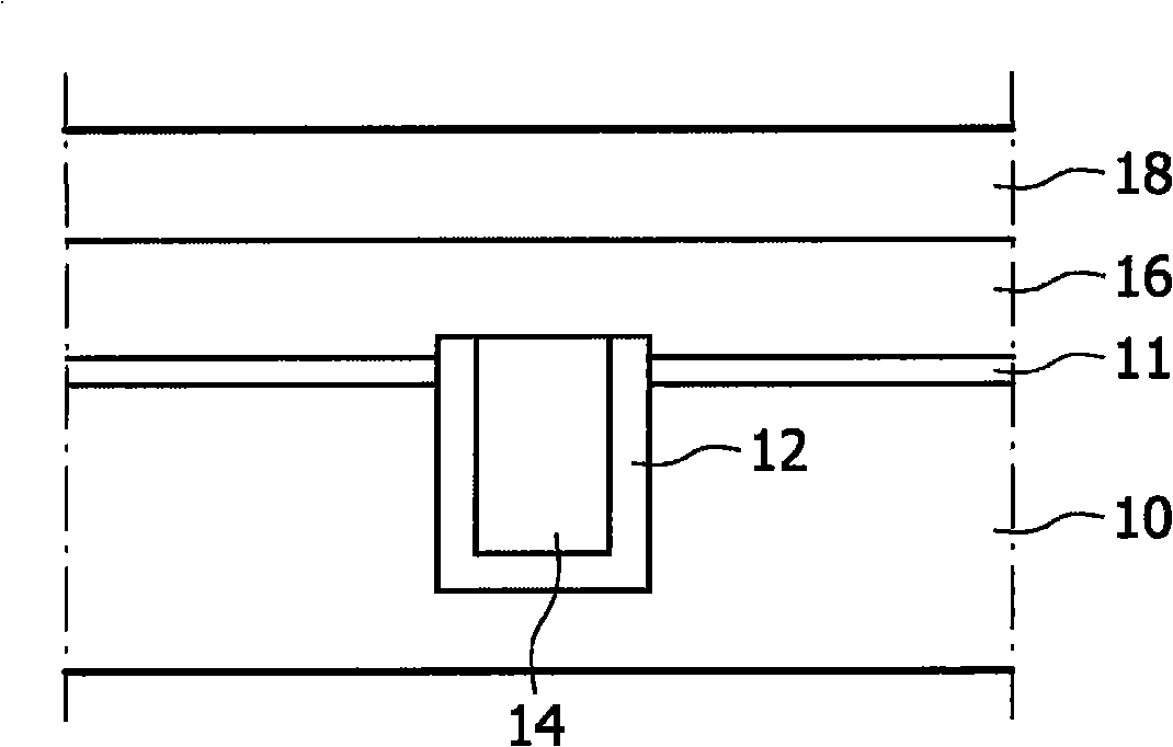
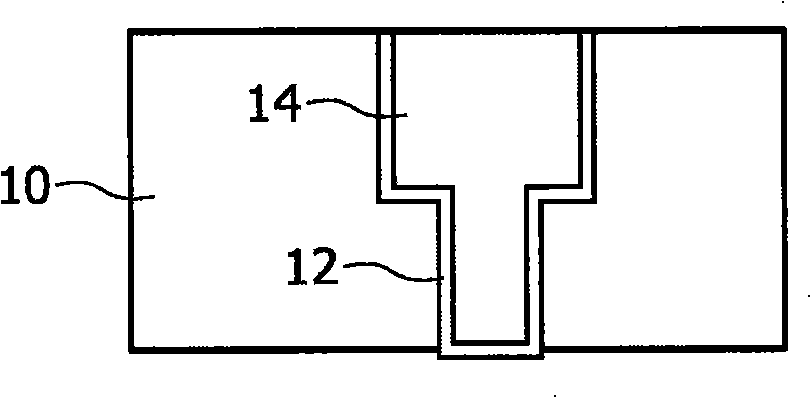
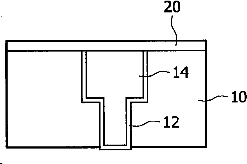
[0036] Starting from the structure after the chemical mechanical polishing step, and referring to the attached Figure 3a and Figure 4a , copper interconnects 14 are embedded within metal-in-dielectric layer 10 with barrier layer 12 therebetween. In a first example embodiment of the present invention, a thin metallic Al (or Mg, B, Zn, etc.) Figure 3b shown. Next, a reactive annealing process is performed in an ammonia environment, or in a nitrogen, oxygen, or carbon-containi...


PUM


Abstract

A method of forming a capping layer on a copper interconnect line (14). The method comprises providing a layer (20) of Aluminium over the interconnect line (14) and the dielectric layer (10) in which it is embedded. This may be achieved by deposition or chemical exposure. The structure is then subjected to a process, such as annealing or further chemical exposure, in an environment containing, for example, Nitrogen atoms, so as to cause indiffusion of Al into the copper line (14) and nitridation to form a diffusion barrier 26 of the intermetallic compound CuAlN.

Description

technical field [0001] The present invention relates to a method for forming a self-aligned copper capping layer associated with a copper interconnect layer of a semiconductor device in order to improve its reliability and to improve capacitive coupling between lines. Background technique [0002] In the past, aluminum was the predominant conductive material used in electrical interconnects in semiconductor devices due to its low resistivity, good adhesion to silicon dioxide, low price, ease of bonding, and good etchability . As device geometries continue to scale down for very large scale integration, there is an increasing need for interconnect routing with fine spacing and high conductivity while requiring higher levels of reliability. Currently, an integrated circuit is considered to be performing well if testing shows an equivalent useful life of 10 years. However, in some specific applications, such as space applications (e.g., satellites, probes, etc.), medical (e.g...

Claims


Application Information

Patent Timeline
Patent Type & Authority Applications(China)
IPC IPC(8): H01L21/768H01L23/532
CPCH01L23/53295H01L2924/0002H01L21/76867H01L21/76856H01L21/76834H01L2924/3011H01L23/53238H01L21/76849H01L21/76886H01L2924/00H01L21/28H01L21/768H01L23/522
Inventor 维姆·F·A·贝斯林托马斯·瓦尼佩
Owner NXP BV
Why Eureka
Try Eureka