
Lateral diffusion metal-oxide-semiconductor element with low opening resistor and manufacturing method thereof

A technology of turn-on resistance and manufacturing method, which is applied in the direction of semiconductor/solid-state device manufacturing, semiconductor devices, electrical components, etc., can solve the problems of decrease of saturation current and increase of turn-on resistance, and achieve reduction of turn-on resistance, increase of saturation current, and easy alignment Effect

Active Publication Date: 2008-12-10
MACRONIX INT CO LTD
View PDF0 Cites 17 Cited by
  • Summary
  • Abstract
  • Description
  • Claims
  • Application Information

AI Technical Summary

Problems solved by technology

However, the formation of the field oxide layer will lead to an increase in the turn-on resistance, resulting in a decrease in the saturation current

Method used


Image

  • Lateral diffusion metal-oxide-semiconductor element with low opening resistor and manufacturing method thereof
  • Lateral diffusion metal-oxide-semiconductor element with low opening resistor and manufacturing method thereof
  • Lateral diffusion metal-oxide-semiconductor element with low opening resistor and manufacturing method thereof

Examples


Embodiment Construction

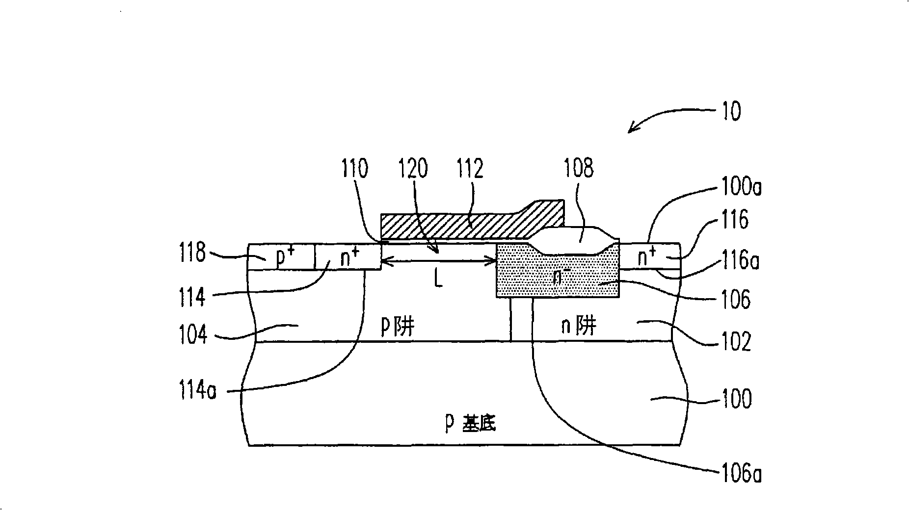
[0023] figure 1 It is a laterally diffused metal oxide semiconductor device according to an embodiment of the present invention.

[0024] Please refer to figure 1 The laterally diffused metal oxide semiconductor element 10 includes an N-type well region 102, a P-type well region 104, an N-type doped region 106, a field oxide layer 108, and an N-type doped region 116 as an N-type drain region and an N-type The doped region 114 serves as an N-type source region, a gate dielectric layer 110 , a gate conductive layer 112 and a P-type base contact region (bulk contact region) 118 .

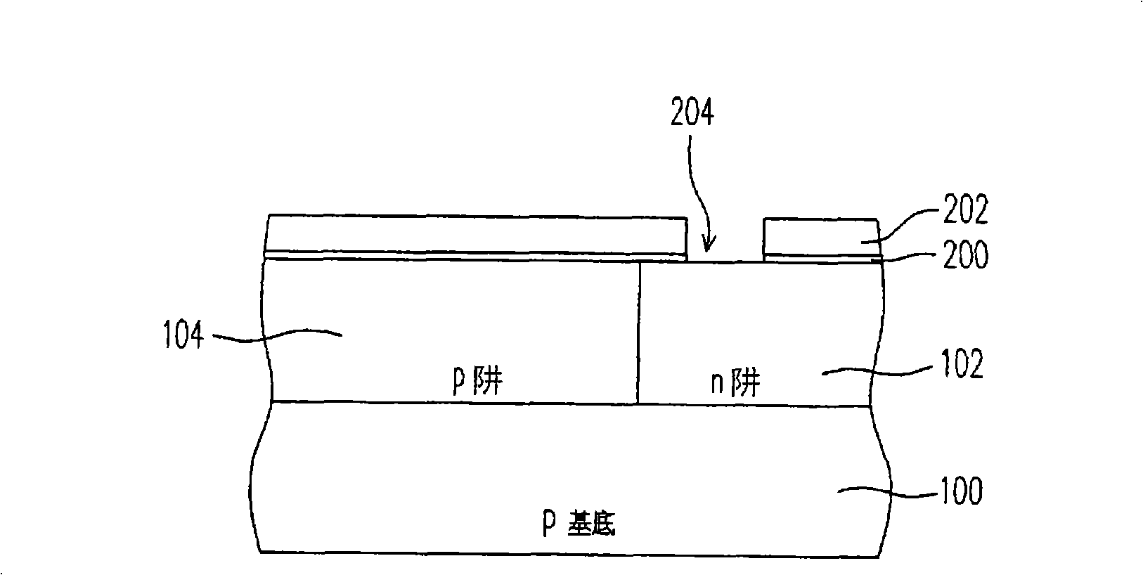
[0025] The N-type well region 102 is adjacent to the P-type well region 104 and both are located in the substrate 100 . The method for forming the N-type well region 102 and the P-type well region 104 can be achieved by forming a photoresist pattern respectively and using an ion implantation preparation process and a drive-in step.

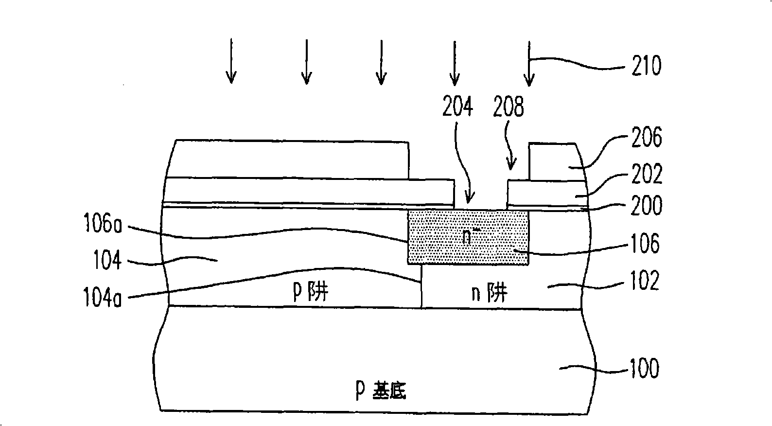
[0026] The source region 114 is located in the P-type well region ...


PUM


Abstract

The invention a transverse diffusion metal-oxide-semiconductor element of a low turn-on resistance, comprising a first well region with a first conduction type, a second well region with a second conduction type, a drain electrode region with the first conduction type, a source electrode region with the first conduction type, a field oxide, a grid dielectric layer, a grid conducting layer and a doping region with the first conduction type. The first well region and the second well region are adjacent and located in a substrate. The drain electrode region is located in the first well region. The source electrode region is located in the second well region. The field oxide is located on the first well region between the source electrode region and the drain electrode region. The grid conducting layer is located on the second well region between the source electrode region and the drain electrode region, and covers partial filed oxide. The grid dielectric layer is located between the grid conducting layer and the substrate. The doping region is located in the first well region below partial grid conducting layer and the field oxide, and is connected with the drain electrode region, wherein the second well region between the doping region below the grid dielectric layer and the source electrode region defines a channel region.

Description

technical field [0001] The present invention relates to an integrated circuit and its manufacturing method, and in particular to a low turn-on resistance lateral diffusion metal oxide semiconductor element and its manufacturing method. Background technique [0002] A laterally diffused metal oxide semiconductor (LDMOS) device is a typical high-voltage device that can be integrated with a complementary MOS process to fabricate control, logic, and power switches on a single chip. The LDMOS device must have a high breakdown voltage (breakdown voltage) and a low on-state resistance (Ron) during operation. LDMOS devices with high breakdown voltage and low on-resistance have lower power loss in high-voltage applications. In addition, the lower on-resistance enables the transistor to have a higher drain current in saturation to increase the operating speed of the device. [0003] The high electric field and high drain current at the drain end of the laterally diffused metal oxide...

Claims


Application Information

Patent Timeline
IPC IPC(8): H01L29/78H01L21/336
CPCH01L29/0847H01L29/42368H01L29/66659H01L29/7835
Inventor 黄学义朱建文林正基连士进叶清本吴锡垣
Owner MACRONIX INT CO LTD
Learn More