Emitter electrode structure capable of improving crystal silicon solar battery shortwave response
A technology of crystalline silicon solar cells and emitters, which can be used in circuits, photovoltaic power generation, electrical components, etc., and can solve problems such as heavy doping of emitters
- Summary
- Abstract
- Description
- Claims
- Application Information
AI Technical Summary
Problems solved by technology
Method used
Image
Examples
Embodiment 1
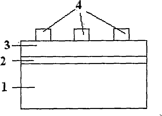
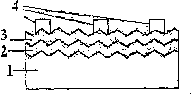
[0019] The emitter structure in this embodiment is as figure 2 As shown, the crystalline silicon substrate 1 is a p-type monocrystalline silicon substrate with a textured surface. On the crystalline silicon substrate 1 is a crystalline silicon layer 2, the crystalline silicon layer 2 is an n-type single crystal silicon layer prepared by diffusion, and the surface doping concentration is 1.0×10 19 / cm 3 , Sheet resistance 200Ω·cm. On the crystalline silicon layer 2 is a transparent conductive electrode layer 3, and the transparent conductive electrode layer 3 is an 80nm thick ITO layer prepared by magnetron sputtering. On the transparent conductive electrode layer 3 are metal grid lines 4, and the metal grid lines 4 are Ag grid lines prepared by thermal evaporation.
Embodiment 2
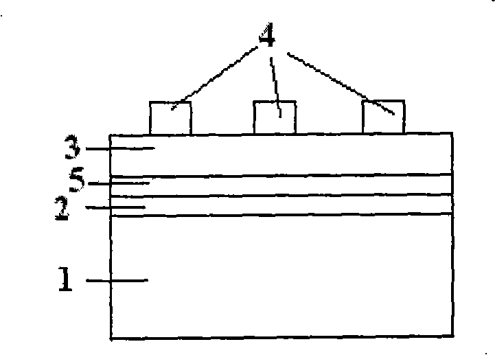
[0021] The emitter structure in this embodiment is as image 3 As shown, the crystalline silicon substrate 1 is an n-type polycrystalline silicon substrate with a flat surface. On the crystalline silicon substrate 1 is a crystalline silicon layer 2, the crystalline silicon layer 2 is a p-type crystalline silicon layer grown epitaxially, and the doping concentration is 1.0×10 20 / cm 3 , Sheet resistance 300Ω·cm. On the crystalline silicon layer 2 is an intrinsic amorphous silicon layer 5, which is prepared by PECVD with a thickness of 1 nm. On the intrinsic amorphous silicon layer 5 is a transparent conductive electrode layer 3, which is an 80nm thick ZnO·Al layer prepared by thermal evaporation. On the transparent conductive electrode layer 3 is a metal grid line 4, and the metal grid line 4 is an Al grid line prepared by magnetron sputtering.
Embodiment 3
[0023] The emitter structure in this embodiment is as Figure 4 As shown, the crystalline silicon substrate 1 is a p-type polycrystalline silicon substrate with a textured surface. On the crystalline silicon substrate 1 is a crystalline silicon layer 2, the crystalline silicon layer 2 is an n-type crystalline silicon layer prepared by diffusion, and the doping concentration is 1.0×10 20 / cm 3 , Sheet resistance 500Ω·cm. On the crystalline silicon layer 2 is an intrinsic amorphous silicon layer 5 prepared by HWCVD with a thickness of 10 nm. The transparent conductive electrode layer 3 is on the intrinsic amorphous silicon layer 5, and the transparent conductive electrode layer 3 is an 80nm thick ZnO·Al layer prepared by electron beam evaporation. On the transparent conductive electrode layer 3 is a metal grid line 4, and the metal grid line 4 is an AgAl alloy grid line prepared by electron beam evaporation.
PUM
| Property | Measurement | Unit |
|---|---|---|
| Thickness | aaaaa | aaaaa |
| Doping concentration | aaaaa | aaaaa |
| Thickness | aaaaa | aaaaa |
Abstract
Description
Claims
Application Information


