Technology for preparing emitting electrode without dead layer by adopting alkaline method and texturization
A preparation process and emitter technology, applied in the field of preparation process of non-dead layer emitter after alkali method, can solve the problems affecting battery efficiency, etc., achieve the effect of improving short-wave response, easy industrial production, and reducing dark current
- Summary
- Abstract
- Description
- Claims
- Application Information
AI Technical Summary
Problems solved by technology
Method used
Image
Examples
Embodiment 1
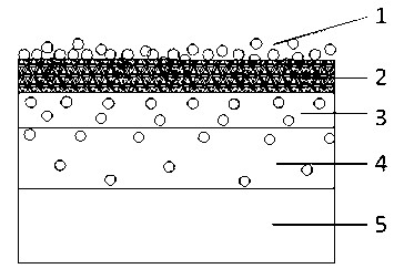
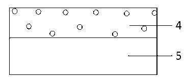
[0028] Put the P-type monocrystalline silicon wafer 5 into a NaOH solution with a temperature of 80°C and a concentration of 180g / L, soak for 20s, and remove the damaged layer on the surface of the silicon wafer 5; then put the silicon wafer 5 into a conventional diffusion furnace, Perform traditional diffusion with a diffusion time of 6 hours to prepare an emitter with a square resistance of 8 ohm / sq; use HF acid solution with a concentration of 10% to remove the silicon glass 2 containing doping sources on the surface of the silicon wafer; Put the silicon wafer 5 of the silicon glass 2 with a concentration of 5g / L and a mixed solution of IPA with a concentration of 150g / L to complete the surface texture for 1000s, and remove the dead layer emitter 3 at the same time. The square resistance of the surface of the silicon wafer 5 without the dead layer emitter 4 is 78 ohm / sq; then put it into a mixed solution of 5% HCl and 7% HF acid for cleaning for 5 minutes. Then the silicon ...
Embodiment 2
[0030] Put the P-type monocrystalline silicon wafer 5 into the NaOH solution with a temperature of 80°C and a concentration of 180g / L, soak for 20s, and remove the damaged layer on the surface of the silicon wafer 5; then put the silicon wafer 5 into a conventional diffusion furnace , carry out traditional diffusion, the diffusion time is 5.5h, and prepare an emitter with a square resistance of 10ohm / sq; use a HF acid solution with a concentration of 10% to remove the silicon glass 2 containing the dopant source on the surface of the silicon wafer; the removed Put the silicon wafer 5 of silicon glass 2 containing the dopant source into a mixed solution of NaOH with a concentration of 5g / L and IPA with a concentration of 150g / L to complete the surface texture for 940s, and remove the dead layer emitter 3 at the same time At this time, the square resistance of the surface of the silicon wafer 5 without the dead layer emitter 4 is 83 ohm / sq; then put it into a mixed solution of 5%...
PUM
 Abstract
Description
Claims
Application Information

