Cadmium telluride solar cell with Te-Ti-Cu pre-set layer
A te-ti-cu, solar cell technology, applied in circuits, photovoltaic power generation, electrical components, etc., can solve problems such as affecting the long-term stability of batteries
- Summary
- Abstract
- Description
- Claims
- Application Information
AI Technical Summary
Problems solved by technology
Method used
Image
Examples
Embodiment 1
[0019] Evaporation method: (1) Preparation of Te-Ti-Cu pre-layer
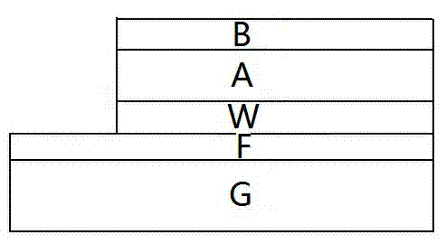
[0020]Put the sample into the vacuum chamber, evacuate, the temperature of the sample is at room temperature, and use the electron beam evaporation method to sequentially deposit tellurium (T1), titanium (T2) and copper (T3), wherein the purity of the raw material tellurium is 99.99% and above, titanium The purity of copper is 99.99% and above, and the purity of copper is 99.99% and above. The thickness of deposited tellurium (T1) is 1~10 nm, the thickness ratio of tellurium (T1) to titanium (T2) is 3.1, and the ratio of copper (T3) to tellurium (T1) thickness is 0.05, so that a period of Te-Ti- The Cu preset layer (B) was continuously deposited for 20 cycles to obtain a Te-Ti-Cu preset layer (B) with a total thickness of 250 nm. After the last cycle of the Te-Ti-Cu preset layer (B), the Deposit titanium with a thickness of about 500nm as the back electrode;
[0021] (2) Post-processing Te-Ti-Cu preset lay...
Embodiment 2
[0024] Sputtering method: (1) Preparation of Te-Ti-Cu pre-layer
[0025] Fix the tellurium target (purity 99.99% and above), titanium target (purity 99.99% and above) and copper target (purity 99.99% and above) respectively on the three target positions corresponding to the sputtering device, and fix the sample on the substrate In terms of position, adjust the distance between the target and the substrate by 6-9 cm; put the sample into the vacuum chamber, evacuate, the sample temperature is at room temperature, and deposit tellurium (T1), titanium (T2) and copper ( T3), where the background vacuum ~10 -4 Pa, the working gas is argon, the working pressure is 0.1~3.5 Pa, the sputtering power of the tellurium target is 30~100 W, the sputtering power of the molybdenum target is 30~300 W, the sputtering power of the copper target is 30~100 W, and the deposition of tellurium (T1) The thickness is 1~10 nm, the thickness ratio of tellurium (T1) and titanium (T2) is 3.1, and the ...
Embodiment 3
[0029] Pulse laser deposition method: KrF excimer laser as excitation source, repetition frequency 1Hz, distance between target and substrate S 4 cm, laser pulse energy density 1~3J / cm 2 , the background air pressure of the growth chamber is 10 -4 Pa, laser irradiates a Te target (99.999%) to grow a Te (T1) film, then laser irradiates a Ti target (99.999%) to grow a Ti (T2) film, and then ablates a copper target (99.999%) to deposit a Cu (T3) film, where The thickness of tellurium (T1) is 1~10 nm, the thickness ratio of tellurium (T1) to titanium (T2) is 3, and the ratio of copper (T3) to tellurium (T1) thickness is 0.05, thus completing a cycle of Te-Ti- Preparation of Cu pre-layer (B). Repeat the above steps more than 20 times to obtain a Te-Ti-Cu preset layer (B) with a total thickness of more than 200 nm. After the last cycle of the Te-Ti-Cu preset layer (B), deposit titanium ( T2) with a thickness of about 500 nm is used as the back electrode; the post-treatment of the...
PUM
| Property | Measurement | Unit |
|---|---|---|
| Thickness | aaaaa | aaaaa |
| Thickness | aaaaa | aaaaa |
Abstract
Description
Claims
Application Information


