High-performance OLED light emitting device

A technology of electroluminescent devices and light-emitting layers, which is applied in the field of OLED light-emitting devices, and can solve problems such as affecting the life of OLED devices, large HOMO energy level difference, and hindering effective hole injection.

Active Publication Date: 2020-04-03
JIANGSU SUNERA TECH CO LTD
View PDF4 Cites 0 Cited by
  • Summary
  • Abstract
  • Description
  • Claims
  • Application Information

AI Technical Summary

Problems solved by technology

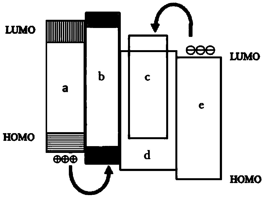
[0006] etc., there is a large difference between the HOMO energy level and the HOMO energy level of the main material of the light-emitting layer, and it is easy to form accumulated charges at the material interface, which affects the life of the OLED device.
[0007] In addition, in organic electroluminescent devices, not all the energy levels of the materials are well matched, and the potential barriers between them seriously hinder the efficient injection of holes.

Method used


Image

  • High-performance OLED light emitting device
  • High-performance OLED light emitting device
  • High-performance OLED light emitting device

Examples


Embodiment 1

[0075] Embodiment 1 prepares compound HI-3

[0076]

[0077] Under nitrogen atmosphere, add 0.01mol raw material A1, 0.012mol raw material B1, 0.02mol sodium tert-butoxide, 1×10 -4 mol Pd 2 (dba) 3 and 1×10 -4 mol of tri-tert-butylphosphine, then add 150ml of toluene to dissolve it, heat to 100°C, reflux for 24 hours, observe the reaction by TLC until the reaction is complete. Naturally cooled to room temperature, filtered, and the filtrate was rotary evaporated until there was no fraction. The obtained substance was purified by a silica gel column (the volume ratio of petroleum ether and dichloromethane was 2:1 as eluent) to obtain the target product with a purity of 99.0% and a yield of 66.2%.

[0078] Elemental analysis structure (molecular formula C 54 h 37 N): theoretical value, C, 92.67; H, 5.33; N, 2.00; test value: C, 92.66; H, 5.35; N, 2.01. ESI-MS(m / z)(M + ): The theoretical value is 699.29, and the measured value is 699.50.

Embodiment 2

[0079] Embodiment 2 prepares compound HI-8

[0080]

[0081] According to the synthetic method of compound HI-3, the difference is that raw material A1 is replaced by raw material A2, raw material B1 is replaced by raw material B2, the purity of the obtained target product is 99.91%, and the yield is 73.7%.

[0082] Elemental analysis structure (molecular formula C 48 h 12 D. 21 N): theoretical value, C, 89.39; H, 8.43; N, 2.17; tested value: C, 89.37; H, 8.45; N, 2.19. ESI-MS(m / z)(M + ): The theoretical value is 644.39, and the measured value is 644.59.

Embodiment 3

[0083] Embodiment 3 prepares compound HI-16

[0084]

[0085] It was prepared according to the synthetic method of compound HI-3, except that raw material A3 was used instead of raw material A1, and raw material B3 was used instead of raw material B1. The purity of the obtained target product was 99.84%, and the yield was 70.1%.

[0086] Elemental analysis structure (molecular formula C 60 h 42 N 2 ): theoretical value, C, 91.11; H, 5.35; N, 3.54; test value: C, 91.13; H, 5.36; N, 3.54. ESI-MS(m / z)(M + ): The theoretical value is 790.33, and the measured value is 790.57.


PUM

PropertyMeasurementUnit
thicknessaaaaaaaaaa
thicknessaaaaaaaaaa
thicknessaaaaaaaaaa

Abstract

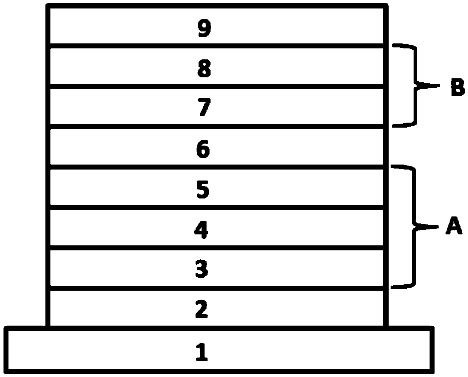
The invention discloses a high-performance OLED light emitting device. The light emitting device comprises a first electrode, an anode interface buffer layer, a hole transport layer, a luminescent layer and a second electrode, wherein the anode interface buffer layer covers the surface of the electrode, the hole transport layer is adjacent to the interface buffer layer, the anode interface bufferlayer contains a hole-conducting main body material and a P-doped material, and the HOMO energy level of the hole-conducting main body material is greater than that of the hole transport layer material. Through the design of the interface buffer layer, the hole injection efficiency from the electrode to the organic material can be improved, the interface conduction barrier difference of carriers from the buffer layer to the hole transport layer is reduced or eliminated, the interface stability of the anode interface buffer layer and the hole transport layer is improved, and the driving stability of the OLED light-emitting device is further improved.

Description

technical field [0001] The invention relates to the technical field of semiconductors, in particular to an OLED light-emitting device with an anode interface buffer layer and a hole transport layer as main functional layers. Background technique [0002] Organic electroluminescent device technology can be used to manufacture new display products, and can also be used to prepare new lighting products. It is expected to replace the existing liquid crystal display and fluorescent lighting, and has a wide application prospect. The organic electroluminescent device is a current device. When a voltage is applied to the electrodes at its two ends, and the electric field acts on the positive and negative charges in the film layer of the organic layer functional material, the positive and negative charges are further recombined in the organic light-emitting layer, that is, an organic electroluminescent device is generated. Electromechanical Luminescence. [0003] Organic electrolumi...

Claims


Application Information

Patent Timeline
Patent Type & Authority Applications(China)
IPC IPC(8): H01L51/50H01L51/54
CPCH10K85/60H10K85/624H10K85/622H10K85/636H10K85/626H10K85/633H10K85/615H10K85/631H10K85/6574H10K85/657H10K50/11H10K2101/40H10K85/6572H10K50/155H10K50/15H10K50/17
Inventor 李崇蔡啸张兆超谢丹丹
Owner JIANGSU SUNERA TECH CO LTD
Why Eureka
Try Eureka