Preparation method of selective doping structure of solar cell
A solar cell and selective technology, applied in the field of solar cells, can solve the problems of complex preparation process, prolonged preparation time, complex structure, etc.
- Summary
- Abstract
- Description
- Claims
- Application Information
AI Technical Summary
Problems solved by technology
Method used
Image
Examples
Embodiment Construction
[0033] In order to make the above objects, features and advantages of the present invention more comprehensible, the present invention will be further described in detail below in conjunction with the accompanying drawings and specific embodiments.
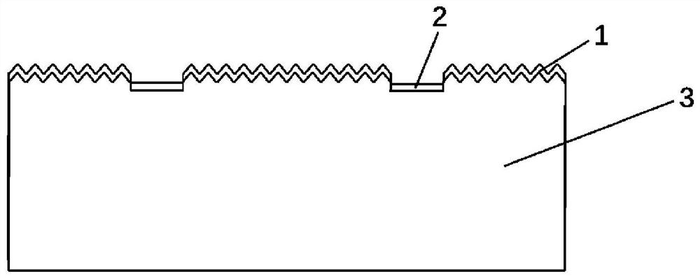
[0034] A method for preparing a selectively doped structure of a solar cell of the present invention comprises the following steps:
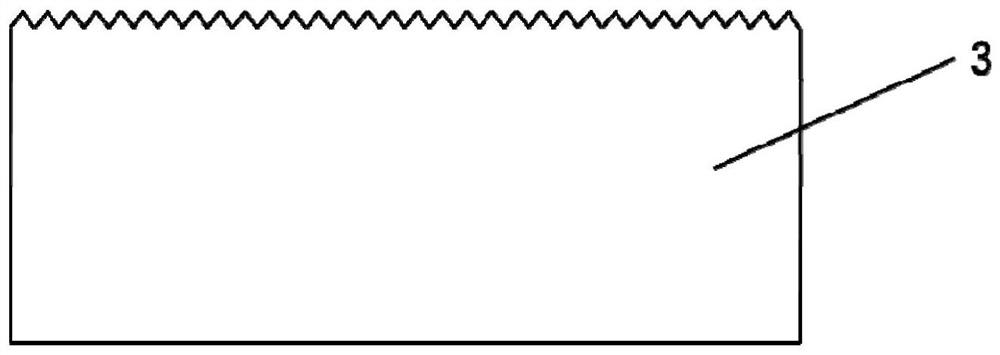
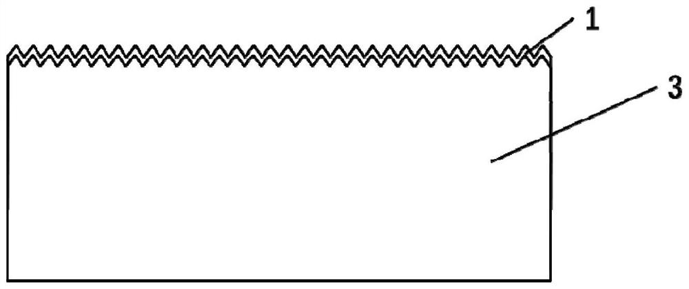
[0035] Step one, see figure 1 , select an N-type silicon wafer 3 with a thickness of 150-180nm and a resistivity of 1-9Ω·cm; after the surface of the silicon wafer 3 is pretreated, deposit dopant containing doping source on the surface of the pretreated silicon wafer 3 Poly layer 1, after the preparation of poly layer 1, its structure is as follows figure 2 shown.
[0036] One of the typical texturing conditions is: the temperature of the rough throwing tank is 75±15°C, the time is 130±50s, the volume fraction of NaOH solution is 2.50%-3.50%; the temperature of the texturing tank is 85±10°C , th...
PUM
| Property | Measurement | Unit |
|---|---|---|
| Thickness | aaaaa | aaaaa |
| Resistivity | aaaaa | aaaaa |
| Thickness | aaaaa | aaaaa |
Abstract
Description
Claims
Application Information


