Method for checking semiconductor substrate crystal quality by linear polarized light

A technology of linearly polarized light and crystal quality, applied in the direction of polarization influence characteristics, optical test flaws/defects, etc., can solve the problems of long preparation period, material destruction, expensive instruments, etc., to achieve low instrument cost and operating cost, improve Yield, material and money savings

Inactive Publication Date: 2009-01-07
NANJING UNIV
View PDF0 Cites 7 Cited by
  • Summary
  • Abstract
  • Description
  • Claims
  • Application Information

AI Technical Summary

Problems solved by technology

However, the instruments used in these methods are very expensive, generally costing more than one million yuan, especially each time only a very limited area can be characterized, and it is impossible to give an intuitive representation of the defect distribution of the entire sheet of material, which is precisely It is especially important for the yield of industrial devices
In addition, using TEM to characterize materials requires a long preparation period for experimental samples, which is not conducive to the rapid development of research work and industrial production; although the method of wet etching is simple, it has irreversible damage to materials.
The number of materials produced as a research is very limited in each batch, and materials such as GaN and SiC bulk materials are very expensive, so this method also has limitations in application

Method used


Image

  • Method for checking semiconductor substrate crystal quality by linear polarized light
  • Method for checking semiconductor substrate crystal quality by linear polarized light

Examples


Embodiment Construction

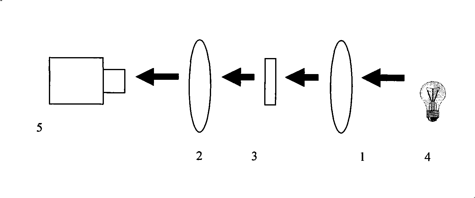
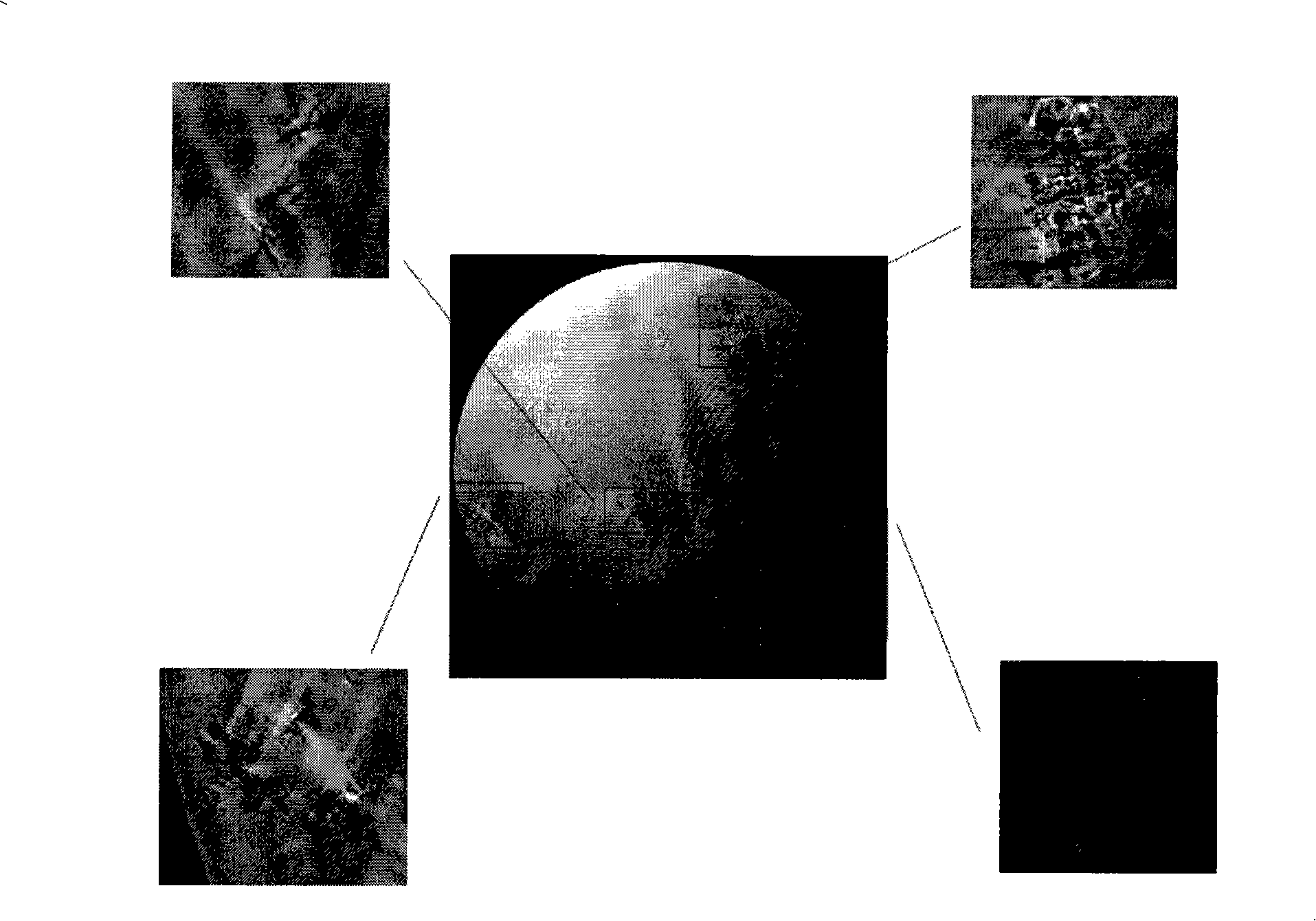
[0015] To further illustrate the content of the present invention, the present invention will be described in detail below in conjunction with the embodiments and accompanying drawings. Among them: see figure 1 As shown, the working process of the method for inspecting the quality of semiconductor substrate crystals using linearly polarized light is:

[0016] 1) A light source 4 is used to generate light of uniform intensity, which light must be able to partially pass through the crystal material 3;

[0017] 2) The light is irradiated vertically on the linear polarizer 1 to generate linearly polarized light;

[0018] 3) The linearly polarized light is irradiated on the 2-inch whole SiC material, and a part of the light is transmitted through the material;

[0019] 4) The transmitted light passes through the linear polarizer 2, and its polarization direction is perpendicular to the linear polarizer 1;

[0020] Finally, it is received and displayed by the optical imaging syst...


PUM


Abstract

The invention relates to a method which adopts linear polarized light to test the quality of semiconductor substrate crystal. Two linear polaroids are arranged vertically in the direction of polarization, in the state of complete extinction. A flake crystal material with a flat surface, which requires defect representation, is arranged between the two polaroids; the plane of the crystal material is parallel to the planes of the two polaroids; a light source is used for producing light of uniform strength which vertically irradiates on one linear Polaroid to product linear polarized light; the linear polarized light irradiates the crystal material again; the transmitted light is ultimately received and displayed by an optical imaging system after passing through the second Polaroid; the image displayed in the optical imaging system has areas with brightness contrast or fringes, which correspond to the defects in the crystal material. Compared with the traditional defect representation, the method can conveniently and directly represent the distribution of the defects of the whole crystal material, which accelerates the research speed and improves the yield of device preparation.

Description

1. Technical field [0001] The invention relates to a method and a device for inspecting the crystal quality of a semiconductor substrate, in particular to a method and a device for inspecting the crystal quality of a semiconductor substrate by using linearly polarized light. 2. Background technology [0002] The quality of a semiconductor crystal material depends largely on its defect density. A higher defect density will seriously reduce the quality of the material, as well as the optical or electrical performance of the device made of the material. Therefore, it is usually desirable to prepare crystalline materials with as low a defect density as possible. Then, effective material defect characterization methods are essential in the process of semiconductor material preparation. At present, there are many methods for characterization of defects in semiconductor crystal materials. Taking the defect characterization of compound semiconductor materials as an example, commonl...

Claims


Application Information

Patent Timeline
Patent Type & Authority Applications(China)
IPC IPC(8): G01N21/88G01N21/21
Inventor 陆海苗操张荣郑有炓
Owner NANJING UNIV
Why Eureka
Try Eureka