LED chip with electrostatic protection function and production method thereof

A LED chip and electrostatic protection technology, which is applied in semiconductor/solid-state device manufacturing, circuits, electrical components, etc., can solve the problems of poor high-voltage electrostatic resistance, insufficient high-voltage resistance of LED chips, scrapping, etc., and achieve the effect of preventing burning

Inactive Publication Date: 2009-01-14
NANKER GUANGZHOU SEMICON MFG
View PDF0 Cites 8 Cited by
  • Summary
  • Abstract
  • Description
  • Claims
  • Application Information

AI Technical Summary

Problems solved by technology

[0003] From the perspective of LED itself, its theoretical life is very long, but in the process of production and use, due to the existence of high-voltage static electricity, LED chips are prone to scrapping due to insufficient high-voltage resistance.
Therefore, the high-voltage electrostatic resistance of the existing LED chips is not good

Method used


Image

  • LED chip with electrostatic protection function and production method thereof
  • LED chip with electrostatic protection function and production method thereof
  • LED chip with electrostatic protection function and production method thereof

Examples


Embodiment 1

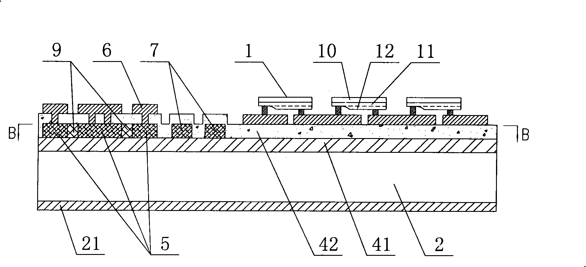
[0054] Such as Figure 1 ~ Figure 4 As shown, the LED chip with electrostatic protection function of the present embodiment includes 12 LED bare chips 1 and silicon substrate 2, and the LED bare chip 1 is a double-electrode chip, and the LED bare chip 1 includes sapphire (Al 2 o 3) substrate 10 and gallium nitride (GaN) N-type epitaxial layer 11, P-type epitaxial layer 12, certainly, described substrate 10 also can be the substrate of other materials such as silicon carbide (SiC), described silicon substrate 2 is a P-type silicon substrate, on which a heat-conducting insulating layer I 41 is formed, and the heat-conducting insulating layer I 41 is composed of a silicon nitride layer. The thermal conductivity of silicon nitride is very high, and its thermal conductivity is higher than The general heat conduction adhesive is more than 100 times higher, and the thickness of the heat conduction insulating layer I 41 is thin simultaneously, so thermal conductivity is good, can pla...

Embodiment 2

[0067] Such as Figure 5 ~ Figure 8 As shown, the difference between this embodiment and Embodiment 1 is that the LED bare chip 1 in the LED chip with electrostatic protection function of this embodiment is a single-electrode chip, and the LED bare chip 1 includes gallium arsenide (GaAs) Substrate 10 and N-type epitaxial layer 11, P-type epitaxial layer 12, certainly, described substrate 10 also can be the substrate of other materials such as silicon carbide (SiC), and each described LED bare chip 1 is loaded on each described on and through the metal layer 6 to form a full-series LED circuit, the substrate 10 is glued on the metal layer 6 with silver paste or tin, and the electrode contacts of the LED bare chip 1 pass through A metal wire is welded on an adjacent metal layer 6 . A layer of N+ diffusion layer 3 is diffused inwardly from the front side of the silicon substrate 2 , and the heat conducting and insulating layer I 41 is grown on the N+ diffusion layer 3 . There a...

Embodiment 3

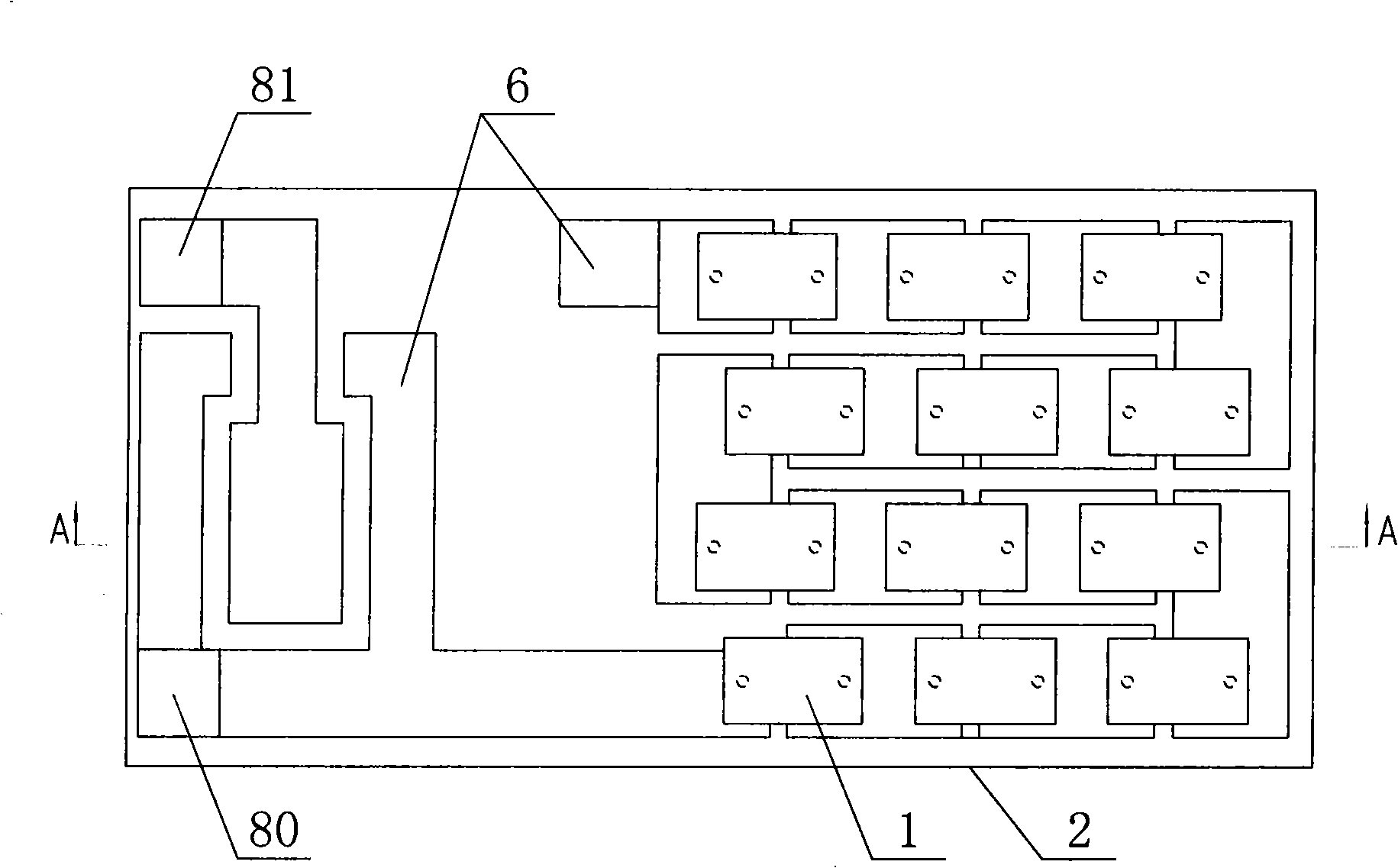
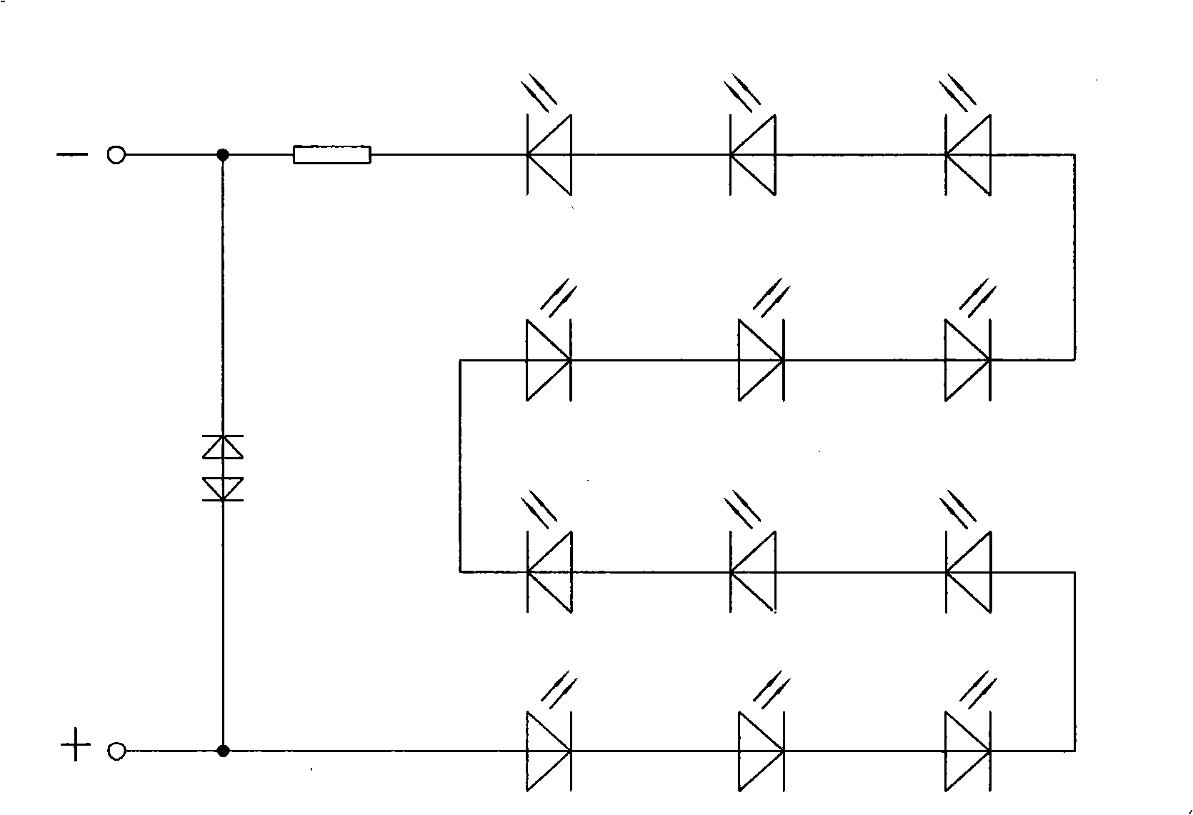
[0075] Such as Figure 9 ~ Figure 12 As shown, the difference between this embodiment and the second embodiment is that: the LED bare chip 1 is a double-electrode chip, and the substrate 10 is aluminum oxide (sapphire, Al 2 o 3 ) substrate, the P-type epitaxial layer 12 and the N-type epitaxial layer 11 are respectively welded to two adjacent separated metal layers 6 through two metal wires. There are two resistance areas 7, one end of the two resistance areas 7 are respectively connected to the anode contact 80 and the cathode contact 81 in ohm, and the other ends of the two resistance areas 7 are connected in series In the LED bare chip 1, each of the electrostatic protection diode regions is formed with a polarity of N + PN + PN + Zener diode groups, two of the Zener diode groups are connected in parallel between the positive and negative poles on both sides of the delay on-resistance formed by the two resistance regions 7, which has a delay to the LED chip When the co...


PUM


Abstract

The invention provides an LED chip which resists high voltage and has good static performance and static protection function, and a preparation method used for the LED chip. The chip comprises an LED naked chip and a silicon substrate; a heat conduction insulated layer I (41) and a heat conduction insulated layer II (42) are respectively generated on the silicon substrate; a metal layer (6) is deposited on the heat conduction insulated layer II (42); all LED naked chips are positively or reversely arranged on the metal layer (6); a static protection diode area formed by a doped multi-crystal silicon is arranged between the heat conduction insulated layer I (41) and the heat conduction insulated layer II (42) and comprises a multi-crystal silicon ring I (9) and a multi-crystal ring II (5); the multi-crystal silicon ring II(5) is positioned at a central ring and an external-most ring; the multi-crystal silicon ring II (5) and the multi-crystal silicon ring I(9) are mutually embedded intermittently; and the LED naked chip and the static protection diode area are connected with each other by the metal layer (6) so as to form a static protection circuit. The method of the invention comprises the following steps of: forming two heat conduction insulated layers, forming a static protection diode area and a metal, and encapsulating. The LED chip and the preparation method of the invention can be widely applied to the field of the LED chip.

Description

technical field [0001] The invention relates to an LED chip with static protection function; in addition, the invention also relates to a manufacturing method of the LED chip with static protection function. Background technique [0002] Front-mount chip technology is a traditional microelectronic packaging technology, which is mature and widely used. At present, the vast majority of LEDs are formal-mounted LEDs. Whether the substrate of the LED bare chip is gallium arsenide or silicon carbide, a layer of metal is plated on the outside of the substrate as an N-type electrode, and it is also used for heat dissipation. A bracket with a reflective cup is used as the cathode, and the P-type epitaxial layer on it is welded to the anode lead through a metal wire. Since the top of the bare chip and the substrate surface are used as one end of the electrode, it is commonly called "single Electrode chip", at present, yellow light and red light LED mostly use this kind of single elec...

Claims


Application Information

Patent Timeline
Patent Type & Authority Applications(China)
IPC IPC(8): H01L25/00H01L23/488H01L23/60H01L23/36H01L21/48H01L21/50H01L21/60
CPCH01L2224/49107H01L2224/48091H01L2224/73265
Inventor 吴俊纬
Owner NANKER GUANGZHOU SEMICON MFG
Why Eureka
Try Eureka