Method for manufacturing LED directly mounted on a support upside-down

A technology for light-emitting diodes and a manufacturing method, which is applied in semiconductor/solid-state device manufacturing, electrical components, electrical solid-state devices, etc., can solve problems such as inability to meet, restrict miniaturization, and obstruct light output, so as to reduce packaging manufacturing costs and solve the problem of blocking light. problems, the effect of improving reliability

Inactive Publication Date: 2009-01-21
APT ELECTRONICS
View PDF0 Cites 29 Cited by
  • Summary
  • Abstract
  • Description
  • Claims
  • Application Information

AI Technical Summary

Problems solved by technology

Soldering gold wires requires a pad of a certain size. Both the pad area and the gold wire hinder light output, and as the size of the LED becomes smaller and smaller, the influence of the pad and the gold wire becomes more and more significant, which restricts the further miniaturization of the LED. Unable to meet the needs of the market

Method used


Image

  • Method for manufacturing LED directly mounted on a support upside-down
  • Method for manufacturing LED directly mounted on a support upside-down
  • Method for manufacturing LED directly mounted on a support upside-down

Examples


Embodiment approach 1

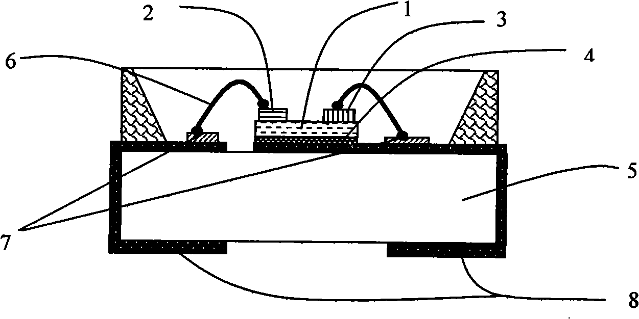
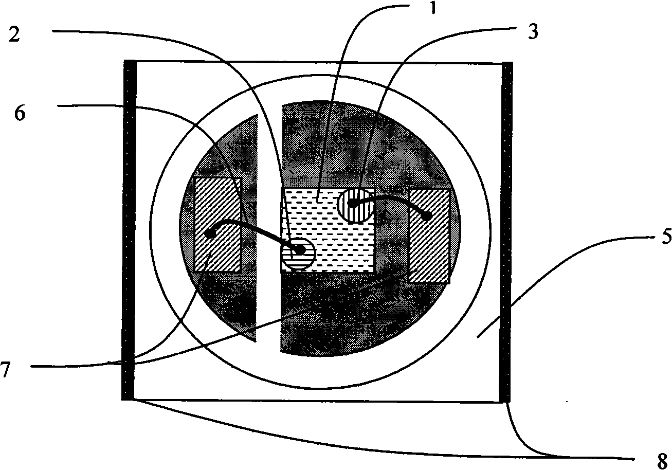
[0033] Aiming at the technology, method and design adopted in the present invention, a surface-mounted top-emitting light bracket for red, green and blue chips is now used, and the bracket material is heat-conducting ceramics. Such as Figure 3-2 and Figure 3-2 As shown, there are three types of LED chips: the blue chip 11 and the green chip 12 are GaN-based, and the red chip 13 is a quaternary chip. The chips of blue light and green light adopt flip-chip technology, and the P electrode and N electrode are on the same side; the red light chip adopts a conventional chip, with the P electrode on the top and the N electrode on the bottom. Die bonding is still required, and then a gold wire 6 needs to be bonded on the P electrode to connect to the pad 7 of the bracket 5 . Both the blue light and the green light chips are directly flipped on the metal bumps 9 corresponding to the bracket 5 through the flip chip technology.

[0034] The production steps are as follows:

[0035]...

Embodiment approach 2

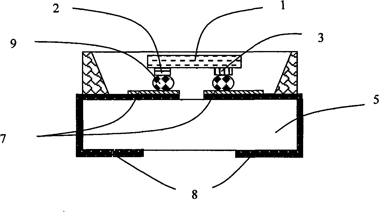
[0041] Aiming at the technology, method and design adopted in the present invention, a surface-mounted side light emitting bracket 5 for a single chip is now used, as shown in Figures 4-3 and 4-4, the bracket material is poly-p-phenylene terephthalamide ( PPA), a white resin material commonly used for stents. The chip is a gallium nitride-based blue LED chip, and the surface of the blue chip is coated with yellow phosphor to form white light. This solution is suitable for small side-emitting LEDs for backlighting. The market requires smaller and smaller package sizes of LEDs, while the demand for brightness is getting brighter. In this way, on the premise that the physical size of the bracket cannot be further reduced, the improvement of the chip is very important.

[0042] The production steps are as follows:

[0043] The first step is to design and manufacture the side-emitting SMD bracket 5 . The external dimensions of the bracket 5 used and the size of the cup mouth ar...


PUM


Abstract

The invention relates to a process for preparing a luminescent diode which is directly and inversely installed in a support, in a support, a single chip or a plurality of chips are directly and inversely installed on the support through metallic salient points. The method saves the steps of fixing a wafer by a chip and bonding by a gold wire, thereby the manufacturing cost is reduced, and the manufacturing efficiency is improved, the heat resistance is reduced, and the heat dissipating problem of a power type chip is solved, the light trapping problem of a bonding pad and a lead wire during the packing of a small size LED is solved, and the luminous efficiency of the LED is greatly improved, the more miniaturization of the packing size of the LED is realized, and the increased requirements of the market to the miniaturization packing are satisfied.

Description

technical field [0001] The invention relates to the field of manufacture and assembly of light-emitting diodes, in particular to a method for manufacturing light-emitting diodes that are directly flipped into a bracket. Background technique [0002] The structure of a conventional gallium nitride-based (GaN) light-emitting diode (LED) is made by forming multiple epitaxial crystal layers of gallium nitride on a sapphire substrate. Such as Picture 1-1 and Figure 1-2 As shown, metal electrodes: P electrode 2 and N electrode 3 are respectively formed on the P-type region and the N-type region of the LED chip 1 . The usual assembly method of traditional light-emitting diode LEDs is to mount and fix the LED chip in the packaging bracket 5 with a thermal interface material (TIM) 4, and connect the metal electrodes 2 and metal electrodes on the LED device through gold wire 6 bonding (Wire Bonding). The electrode 3 and the pad 7 of the package holder. Wherein, the metal electrod...

Claims


Application Information

Patent Timeline
Patent Type & Authority Applications(China)
IPC IPC(8): H01L21/60H01L33/00
CPCH01L2924/01322H01L2924/01029H01L2924/0105H01L2924/01078H01L2924/01028H01L2224/45144H01L2924/01079H01L2224/48091H01L2224/48463H01L2924/01013H01L2224/16H01L2224/48227
Inventor 陈海英罗珮璁肖国伟陈正豪
Owner APT ELECTRONICS
Why Eureka
Try Eureka